


HDI & any-layer
Laser-drilled microvias, stacked & staggered vias and sequential lamination for dense, high-pin-count designs.
Blind/buried to 18+ layers
High-precision multilayer rigid PCB fabrication for industrial, power, RF, automotive, and communication electronics.
Get Instant Rigid PCB QuoteTwo capability tiers — Mass Production for repeatable, high-yield volume, and an extended Prototype window for pushing the limits. Need something beyond these? Ask us — we build to spec.
| Parameter | Mass production | Prototype (extended) |
|---|---|---|
| Layer count | 1–24 layers | 1–78 layers |
| Max. panel size | 600 × 770 mm (23.62″ × 30.31″) | 600 × 770 mm & 500 × 1200 mm (19.69″ × 47.24″) |
| Max. board thickness | 8.5 mm | 8.5 mm |
| Min. board thickness | 2L: 0.3 mm · 4L: 0.4 mm · 6L: 0.8 mm | 2L: 0.1 mm · 4L: 0.3 mm · 6L: 0.6 mm |
| Parameter | Mass production | Prototype (extended) |
|---|---|---|
| Min. inner-layer clearance | 3 mil | 3 mil |
| Min. line width | 3 mil (0.075 mm) | 3 mil (0.075 mm) |
| Min. line space | 3 mil (0.075 mm) | 3 mil (0.075 mm) |
| Parameter | Mass production | Prototype (extended) |
|---|---|---|
| Min. hole size | 0.1 mm | 0.1 mm |
| Min. plated hole copper | 25 µm | 25 µm |
| Min. blind / buried via | 0.1 mm | 0.1 mm (1–18 layers) |
| PTH dia. tolerance | ±0.076 mm (±3 mil) | ±0.076 mm (±3 mil) |
| NPTH dia. tolerance | ±0.05 mm (±2 mil) | ±0.05 mm (±2 mil) |
| Hole position deviation | ±0.05 mm (±2 mil) | ±0.05 mm (±2 mil) |
| Parameter | Mass production | Prototype (extended) |
|---|---|---|
| Heavy copper | 4 oz (140 µm) | up to 12 oz |
| Min. solder-mask bridge | 0.1 mm (4 mil) | 0.1 mm (4 mil) |
| Solder-mask colour | Green, Black, Blue, White, Yellow, Red | Green, Black, Blue, White, Yellow, Red |
| Silkscreen colour | White, Yellow, Red, Black | White, Yellow, Red, Black |
| Peelable mask | Top, bottom, double-sided | Top, bottom, double-sided |
| Parameter | Mass production | Prototype (extended) |
|---|---|---|
| Outline method | Routing, V-groove, beveling, punch | Routing, V-groove, beveling, punch |
| Outline tolerance | ±0.15 mm (±6 mil) | ±0.15 mm (±6 mil) |
| Electrical & reliability | Mass production | Prototype (extended) |
|---|---|---|
| Controlled impedance | ±10% | ±7% |
| Insulation resistance | 1 × 10¹² Ω (normal) | 1 × 10¹² Ω (normal) |
| Through-hole resistance | < 300 Ω (normal) | < 300 Ω (normal) |
| Thermal shock | 3 × 10 sec @ 288 ℃ | 3 × 10 sec @ 288 ℃ |
| Warp & twist | ≤ 0.7% | ≤ 0.7% |
| Electric strength | > 1.3 kV/mm | > 1.4 kV/mm |
| Peel strength | 1.4 N/mm | 1.4 N/mm |
| Solder-mask abrasion | > 6H | > 6H |
| Flammability | 94V-0 | 94V-0 |
| Test voltage | 50–330 V | 50–330 V |

Send your Gerbers and stackup - our engineers confirm manufacturability against this spec and reply with a quote, usually within 24 hours, plus a free DFM review.
Request a QuoteWhen your design pushes the envelope, our advanced process toolkit keeps it manufacturable and reliable.
Laser-drilled microvias, stacked & staggered vias and sequential lamination for dense, high-pin-count designs.
Blind/buried to 18+ layers
High-current and thermal designs with thick inner and outer copper, mixed with fine-line layers.
Up to 12 oz
Single-ended and differential impedance with stackup design support and TDR verification.
Tolerance to ±7%
Removal of via stubs for clean high-speed signal paths in thick multilayer boards.
High-speed designs
Resin- or copper-filled, capped and planarized vias for fine-pitch BGA fan-out.
Plugged & plated over
Castellated / half-plated holes and plated edges for board-to-board and module mounting.
CastellationEvery board is fabricated, inspected and documented to recognized industry standards.

Rigid board - Class 2 & 3

Acceptability of boards

Quality management

Listed 94V-0

EU compliant

Lot & date control

Soldering-ready

Medical-capable

Automotive-capable

Aerospace-capable
Select the solutions that should appear below this capability page.

Bring connected consumer products from prototype to production with XinshunPCB. We support custom PCB fabrication and SMT assembly for wearables, smart-home devices, wireless audio and portable electronics, with material, component and test requirements reviewed around your design.
Explore Solution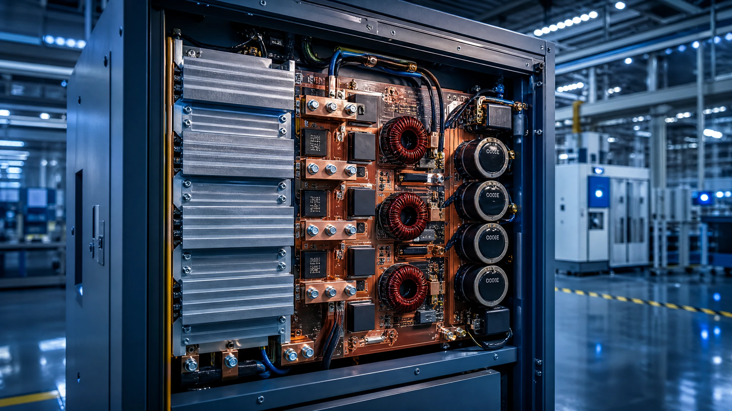
Engineered to withstand massive electrical currents, thermal stress, and continuous mechanical vibration. XinshunPCB delivers IPC Class 3 heavy copper boards, high-thermal metal-core solutions, and turnkey SMT assemblies for grid-scale energy storage, industrial robotics, motor drives, and solar inverters.
Explore Solution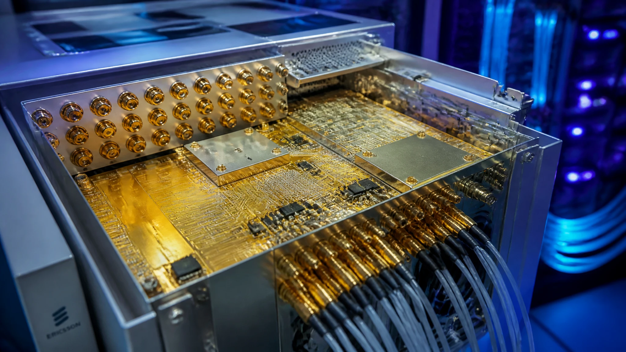
From wireless gateways and connected sensors to networking equipment, XinshunPCB supports custom PCB fabrication and assembly for communication hardware. Align materials, stackups, compact layouts, and production testing with your application, from initial prototypes to repeat production.
Explore Solution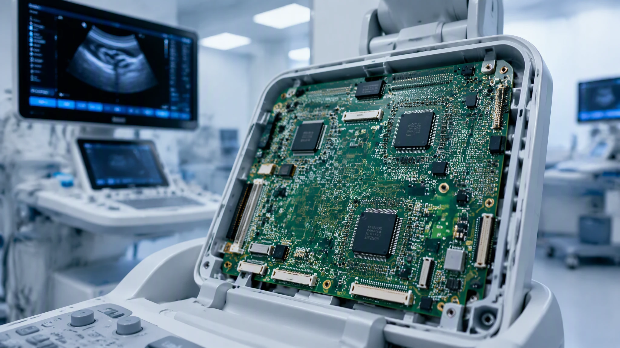
From patient monitoring and diagnostic instruments to medical imaging systems, XinshunPCB provides custom PCB fabrication and PCBA assembly for healthcare equipment. We help you align board materials, circuit layouts, and assembly requirements with your application, supporting development from initial prototypes to production.
Explore Solution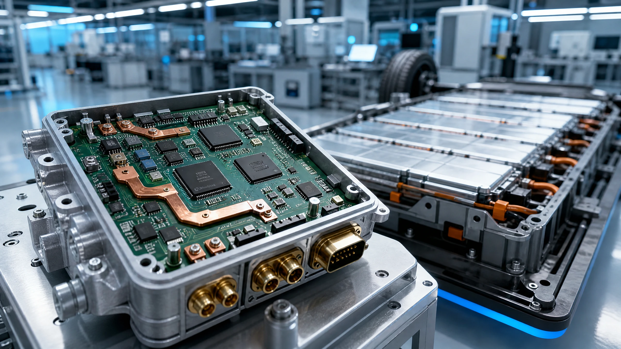
Engineered to withstand extreme mechanical shock, high-voltage switching surges, and thermal cycling from –40°C to +150°C. XinshunPCB delivers IATF 16949-aligned, IPC-A-610 Class 3 turnkey PCB fabrication and SMT assembly for electric vehicle (EV) powertrains, ADAS sensing, high-voltage BMS, and under-hood body control modules.
Explore SolutionSelect the FAQs that should appear below this capability page.

Have a new project or custom PCB requirements? Simply fill in your project details below. XinshunPCB’s FAE engineering team will analyze your specifications and deliver a detailed formal quotation along with free engineering advice within 2–24 hours.
Detailed formal quote & lead time provided within 2-24 hours.

Your contact info and project specs are kept strictly confidential.

Experienced FAE support to help optimize your specifications.
Need a reliable manufacturing partner for your next project? Our global support team is standing by.
Trusted by global integrators for PCB manufacturing, enterprise hardware, and high-reliability deployment solutions.