
Custom HDI PCBs for Dense, Compact Electronics

Custom HDI PCBs for Dense, Compact Electronics

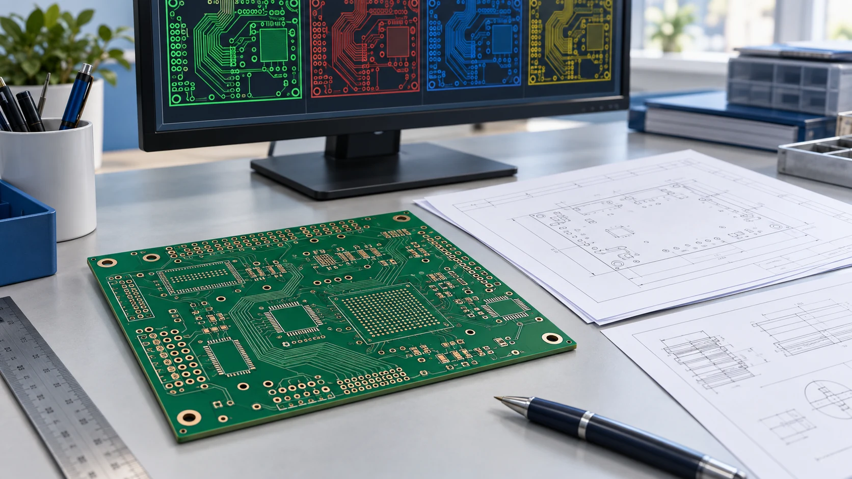
Create routing space for fine-pitch components with high-density interconnect PCBs. XinshunPCB helps align microvias, layer stackups, materials, and assembly requirements for your design, from prototypes to production.

High-Density Interconnects for Your Next Design

Plan fine-pitch routing and layer connections around your component layout, board size, and signal requirements.

Custom High-Density Interconnect PCBs

Custom High-Density Interconnect PCBs

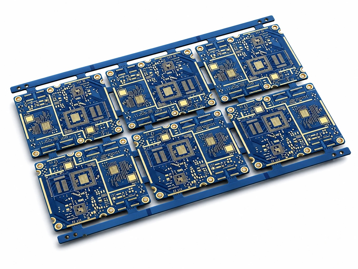
HDI PCBs use fine circuit features and small interlayer connections to route complex designs within limited board space. XinshunPCB reviews your component layout, microvia map, build-up structure, and material requirements together to help prepare a manufacturable construction for your product.

  • Microvia and via-in-pad options for dense component layouts
  • Stackup and material review for routing and signal requirements
  • Prototype evaluation and production planning for your HDI design
Request an HDI PCB Quote

Explore Our HDI PCB Products

Browse selected HDI PCB builds and review their materials, construction, and application details. Use these examples to discuss routing density, layer connections, and assembly needs for your project with XinshunPCB.

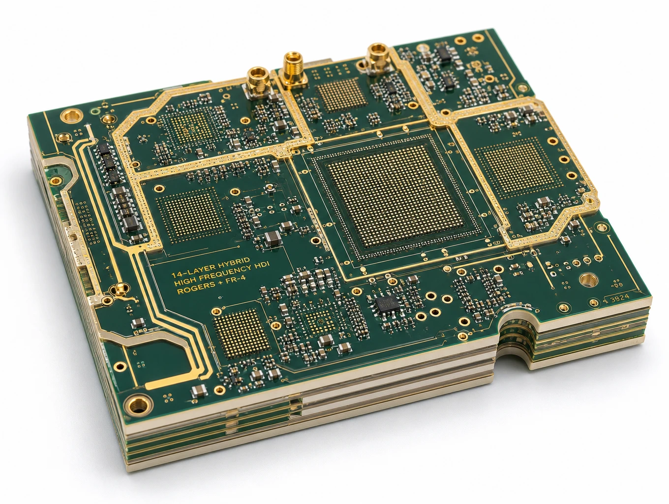
14L High-Speed Hybrid HDI PCB (Rogers + High-TG FR-4)

14L High-Speed Hybrid HDI PCB (Rogers + High-TG FR-4)

  • Layer Count: 14 Layers (Hybrid HDI Stackup)
  • Base Material: Rogers RO4350B / RO4835 (RF Layers) + Shengyi S1000-2M (Internal FR-4 Layers)
  • Application: 5G/6G microwave transceivers, satellite phased-array antenna controllers, aerospace phased telemetry, and high-frequency RF test equipment.
6L 1+N+1 Compact HDI PCB for Medical Endoscopy

6L 1+N+1 Compact HDI PCB for Medical Endoscopy

  • Layer Count: 6 Layers (1+4+1 Stackup)
  • Base Material: Shengyi S1000-2 / TU-872 High-TG FR-4 (Ultra-Thin Core Options)
  • Application: Video endoscopy camera tips, wireless capsule endoscopy, minimally invasive surgical probes, and wearable biometric monitoring patches.
8L 2+N+2 Microvia HDI PCB for Automotive ADAS Systems

8L 2+N+2 Microvia HDI PCB for Automotive ADAS Systems

  • Layer Count: 8 Layers (2+4+2 Stackup)
  • Base Material: ITEQ IT-180A / Isola 370HR (High-TG ≥ 180°C, Low-CTE)
  • Application: Automotive ADAS forward-facing camera modules, millimeter-wave radar sensor controllers, LiDAR processing units, and automotive cockpit domain controllers.
10L Any-Layer HDI PCB (ELIC) with Stacked Microvias

10L Any-Layer HDI PCB (ELIC) with Stacked Microvias

  • Layer Count: 10 Layers (Any-Layer ELIC)
  • Base Material: Panasonic Megtron 6 / Shengyi S1000-2M (High-TG ≥ 170°C)
  • Application: 5G flagship smartphones, edge AI inference processors, high-end smartwatch mainboards, and compact aerospace flight telemetry units.

HDI PCB specifications

Review HDI structures, microvias, and fabrication parameters for your next design. Values below are planning references; the available combination of layer count, copper weight, hole geometry, and tolerances must be confirmed by XinshunPCB during DFM review before ordering.

HDI structure & microvias

ParameterSpecification
HDI structures1+N+1, 2+N+2, 3+N+3; any-layer subject to review
Laser microvia diameter0.1 mm (4 mil); finer features require review
Microvia capture padDesign reference: from approximately 0.25 mm
Microvia typesStacked, staggered, and skip vias
Via fillCopper-filled; resin-filled, capped, and planarized (VIPPO)
Build-upSequential lamination; multiple build-up layers
Minimum blind / buried viaDesign reference: 0.1 mm within 1–18 layers
Through-hole aspect ratioDesign reference: up to approximately 10:1

Lines, spacing & holes

ParameterMass productionPrototype (extended)
Minimum inner-layer clearance3 mil3 mil
Minimum line width3 mil (0.075 mm)3 mil (0.075 mm)
Minimum line space3 mil (0.075 mm)3 mil (0.075 mm)
Minimum mechanical hole0.1 mm0.1 mm
Minimum plated hole copper25 µm25 µm
PTH diameter tolerance±0.076 mm (±3 mil)±0.076 mm (±3 mil)
NPTH diameter tolerance±0.05 mm (±2 mil)±0.05 mm (±2 mil)
Hole position deviation±0.05 mm (±2 mil)±0.05 mm (±2 mil)

Advanced HDI Processes for Dense, Reliable Interconnects

Combine microvia structures, fine-line routing, and controlled stackups to support miniaturization and high-speed performance. The final process route is reviewed against your design and qualification requirements.

Any-layer HDI

Any-layer HDI

Connections between successive layers can shorten escape routes and free routing space around high-pin-count devices. Select an any-layer structure after reviewing density, layer transitions, and reliability requirements.

Any-layer interconnect
Stacked & filled microvias

Stacked & filled microvias

Copper-filled laser microvias can be arranged in stacked or staggered patterns. Match the arrangement to the layer transitions, available pad area, and agreed qualification plan.

Copper-filled microvias
Via-in-pad (VIPPO)

Via-in-pad (VIPPO)

Filled, capped, and planarized vias allow routing connections within component pads. Define the filling and plating requirements to support fine-pitch BGA assembly.

Filled & plated over
Sequential lamination

Sequential lamination

Successive build-up and lamination stages connect outer routing layers to the core. Review 1+N+1, 2+N+2, and more complex structures against the required routing density.

HDI build-up
Fine-line routing

Fine-line routing

Fine trace geometries help route dense component areas. Select copper thickness and the appropriate imaging and etching process; advanced mSAP requirements need a separate process review.

Fine-pitch routing
High-speed & impedance

High-speed & impedance

Coordinate dielectric materials, trace geometry, and reference planes across the HDI stackup. Define impedance targets and test coupons before releasing the design.

Signal integrity

PCB Capability Families: Core Manufacturing Solutions

Rigid, flex, rigid-flex, HDI, metal-core, and SMT production lines cover a broad range of PCB and PCBA needs.

Consumer Electronics

Consumer Electronics

Custom PCB fabrication and assembly for wearables, smart-home devices, wireless audio and portable electronics. XinshunPCB supports design review, component sourcing and project-specific inspection from prototype to production.

Explore Solutions
Industrial & Power Electronics

Industrial & Power Electronics

High-power BMS, energy storage, and industrial control solutions engineered with heavy copper, high-voltage creepage control, and high-TG materials.

Explore Solutions
Telecommunications & IoT

Telecommunications & IoT

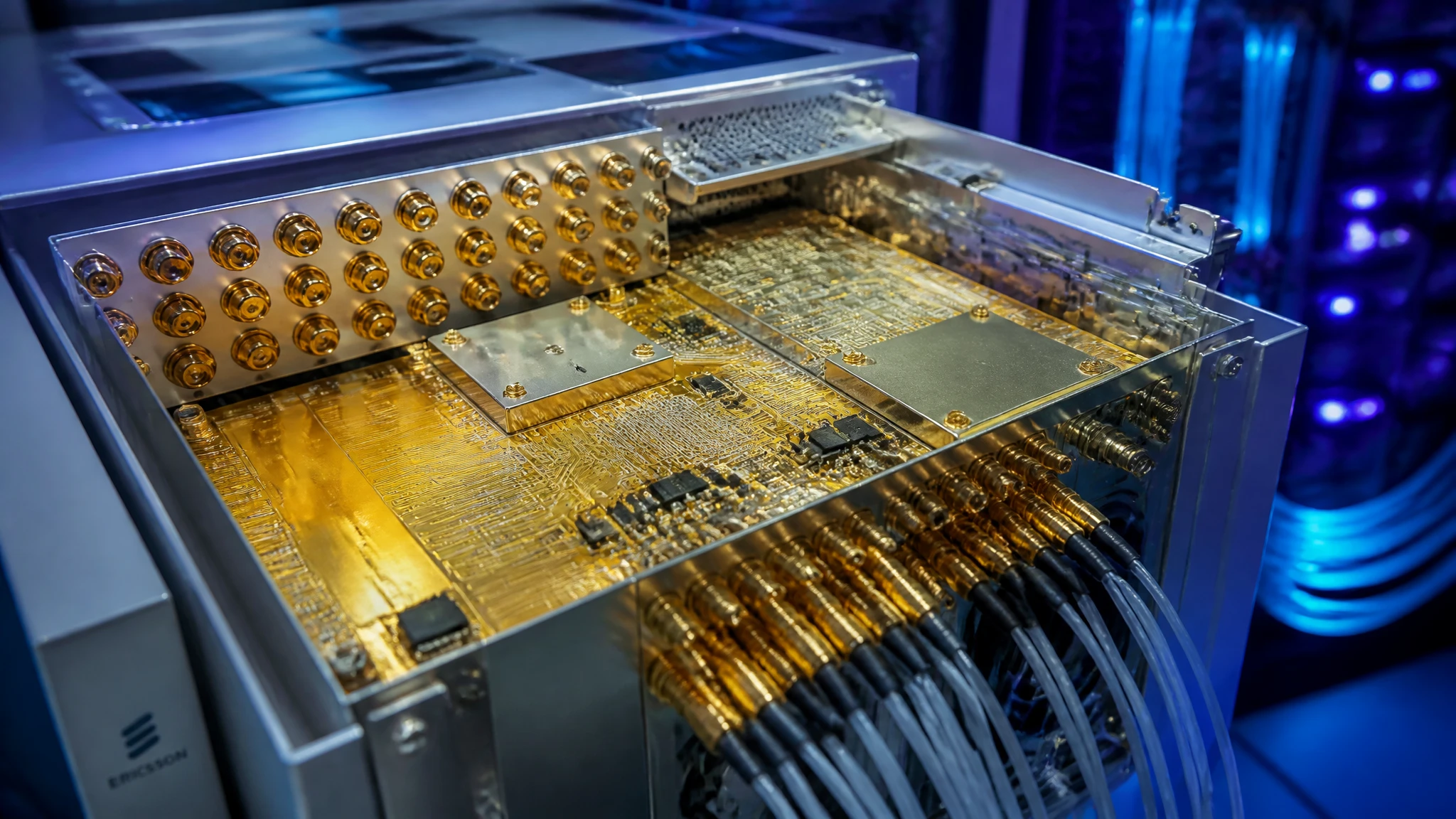
High-frequency PCB and PCBA solutions for RF, 5G, networking, and connected devices.

Explore Solutions
Medical Equipment

Medical Equipment

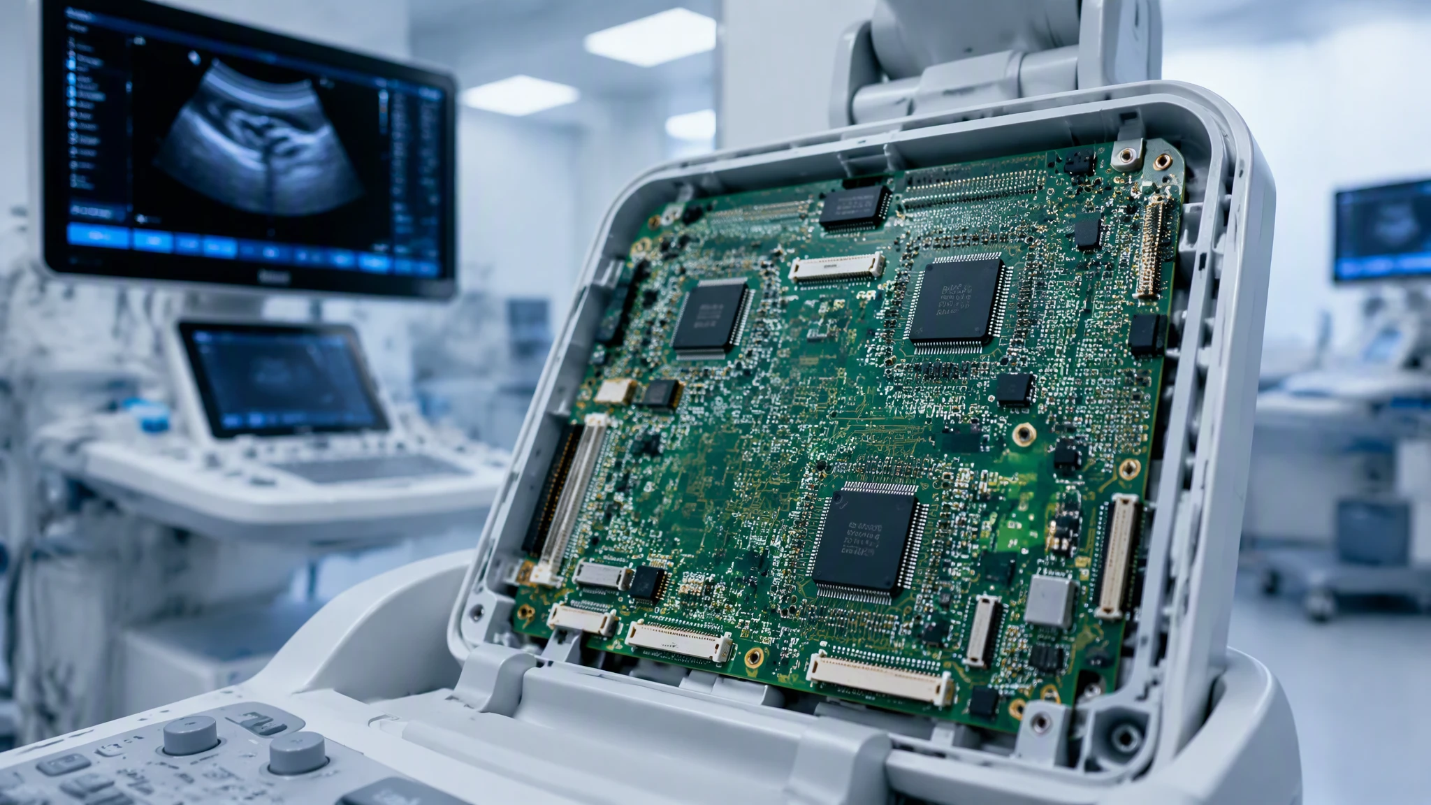
Medical-grade PCB and PCBA solutions built for traceability, reliability, and strict quality control.

Explore Solutions
Automotive Electronic

Automotive Electronic

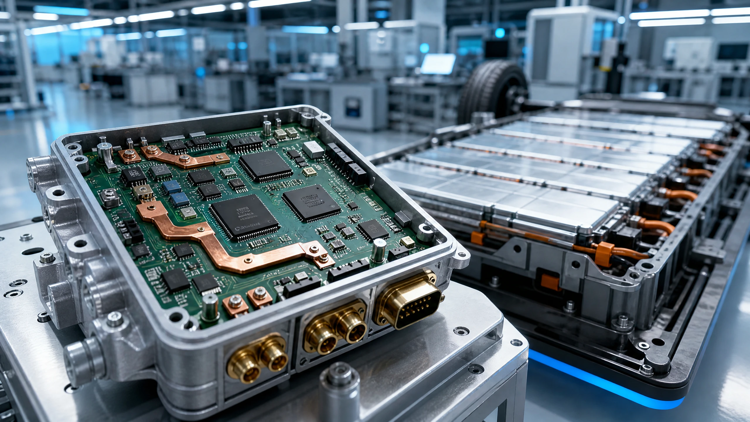
Automotive PCB and PCBA solutions designed for vibration, thermal cycling, and long-life reliability.

Explore Solutions

Frequently Asked Questions About HDI PCBs

Find answers about choosing HDI construction, preparing design files, planning microvias and stackups, and moving from prototype evaluation to production.

Request a prototype build with the intended materials, stackup, and via structure where practical. Use it to evaluate assembly, electrical operation, and fit in the product. Agree the inspection records and any additional reliability or impedance testing before the build. Document the results and release an approved file revision for the next order; production quantities, material availability, and timing are confirmed for each project.

Get Your Custom PCB & PCBA Quote in 24 Hours

Have a new project or custom PCB requirements? Simply fill in your project details below. XINSHUNPCB's FAE engineering team will analyze your specifications and deliver a detailed formal quotation along with free engineering advice within 2-24 hours.

24-Hour Fast Turnaround

Detailed formal quote & lead time provided within 2-24 hours.

100% Privacy & NDA Protection

Your contact info and project specs are kept strictly confidential.

Free Engineering Consultation

Experienced FAE support to help optimize your specifications.

Email WhatsApp