HDI PCB Manufacturing

Committed to providing high-quality products and
professional services to global customers

Home  >  Products  >  HDI Board

HDI PCB Structure and Capabilities

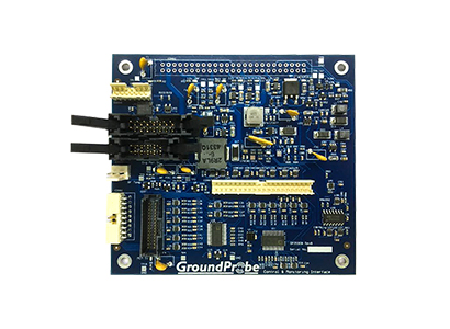
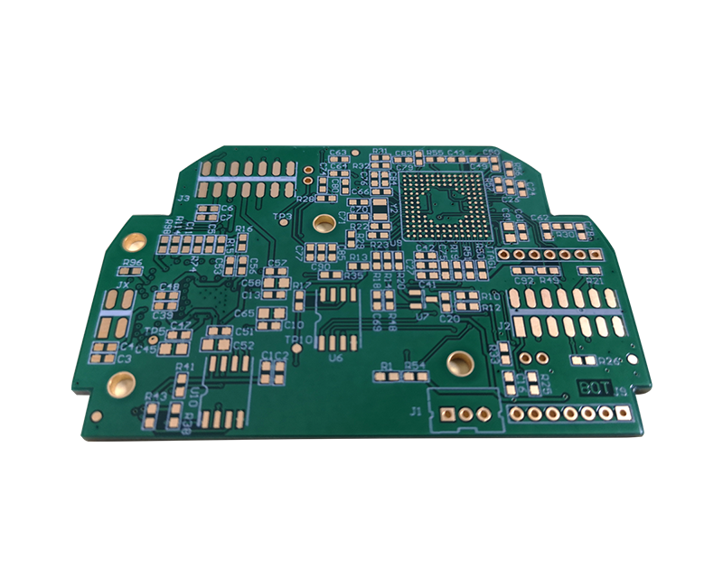
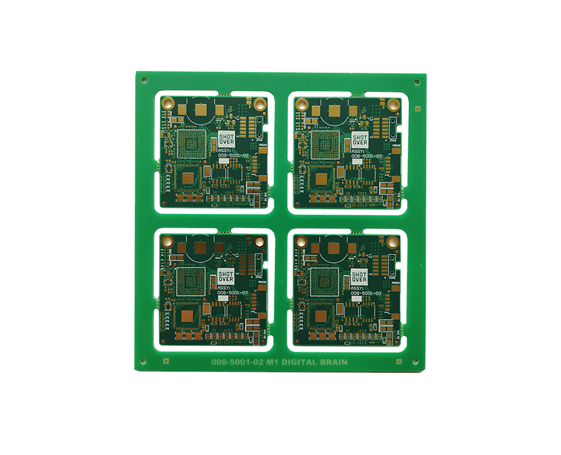
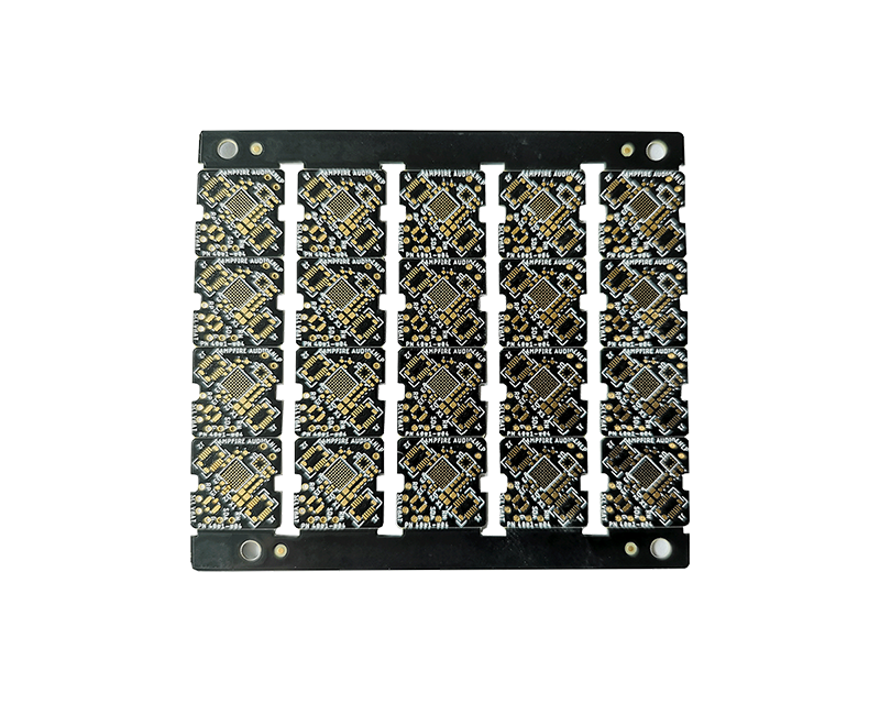
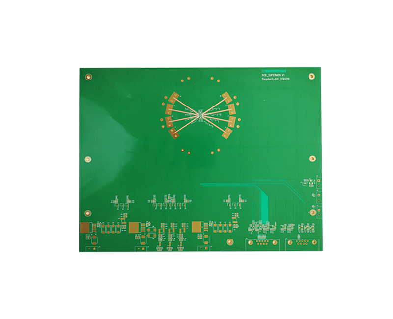
HDI PCB boards are high density interconnect circuit boards designed for compact electronic products that require more routing density, smaller board size and improved signal performance. PCBXINSHUN supports custom HDI PCB manufacturing for multilayer PCB designs with fine lines, microvias, blind vias and buried vias according to customer project requirements.

HDI PCB technology is commonly used in communication devices, industrial electronics, medical equipment, automotive electronics, consumer electronics and other products where space, weight and reliability are important.
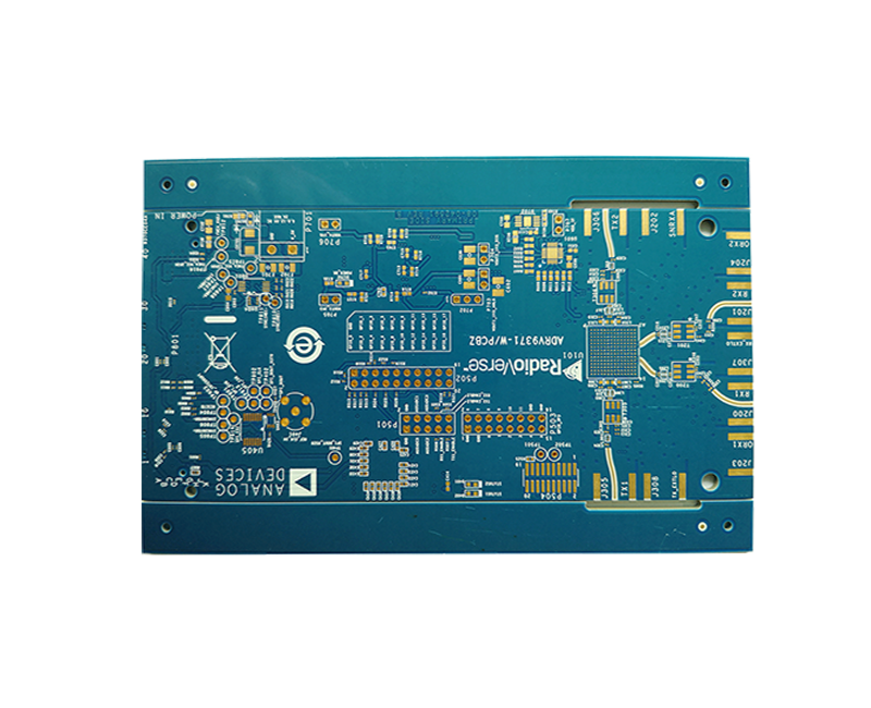
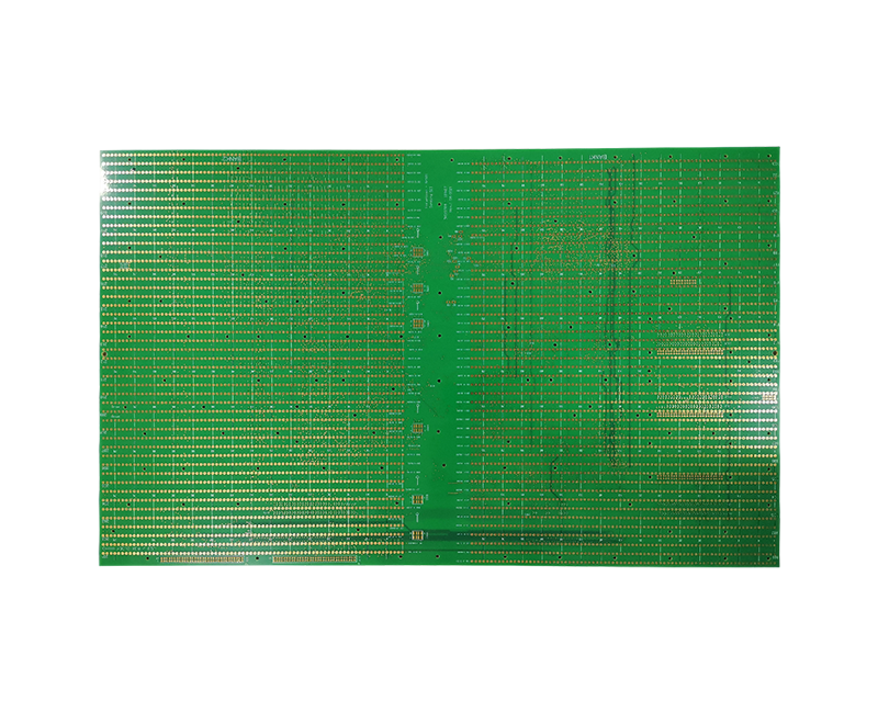
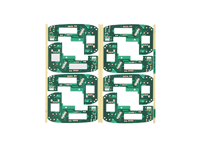
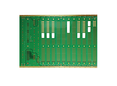
14-layer RO4003C+HTG hybrid board HDI board HDI arbitrary interconnection circuit board

14L, RO4003C+HTG mixed pressure

1-10L, 11-14L blind hole

Blind hole diameter: 0.15mm

Inner yin and yang copper:

1-4L/1-9L layer/0.3mm back drill

Stab:≤2mil, memory space 7mil, resin plug hole

Order Now Know More

PV power:50kW

Energy storage capacity:15.36kWh

Installation location: Singapore

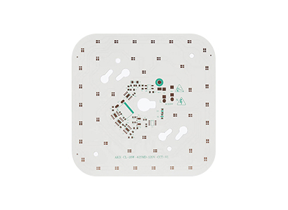
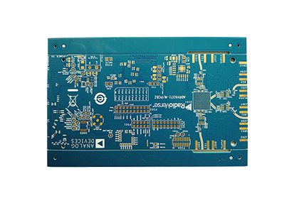
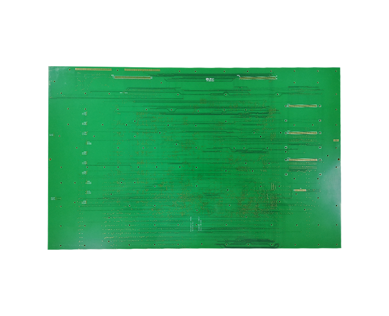
12-layer back drilled board

Order Now Know More

PV power:50kW

Energy storage capacity:15.36kWh

Installation location: Singapore

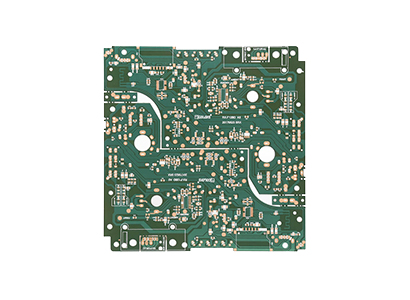
12-layer back drilled board

Order Now Know More

PV power:50kW

Energy storage capacity:15.36kWh

Installation location: Singapore

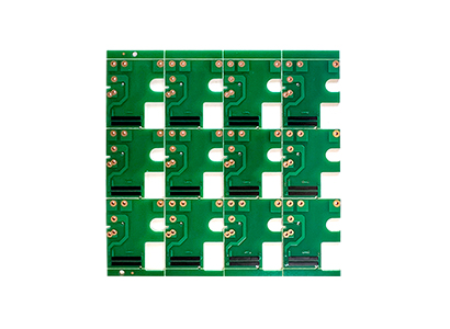
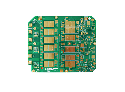
24-layer R5775G (HVLP) back drill board

Order Now Know More

PV power:50kW

Energy storage capacity:15.36kWh

Installation location: Singapore

TLY-5 (PTFE) + high TG mixed pressure, 1+4+1 structure, hole in plate HDI arbitrary interconnection

Order Now Know More

PV power:50kW

Energy storage capacity:15.36kWh

Installation location: Singapore

14-layer RO4003C+HTG hybrid board HDI board HDI arbitrary interconnection circuit board

Order Now Know More

PV power:50kW

Energy storage capacity:15.36kWh

Installation location: Singapore

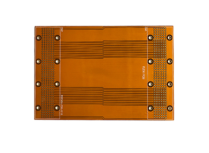
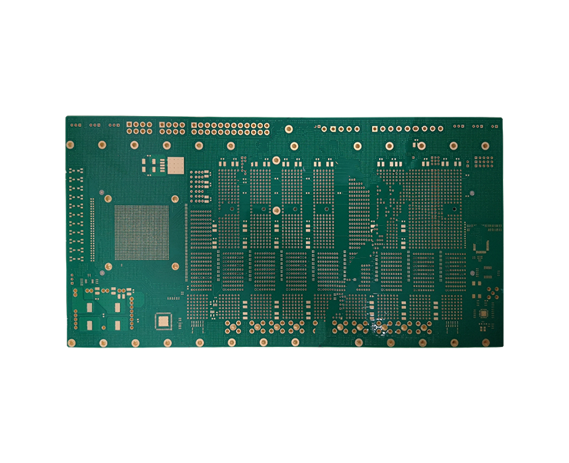
8-layer HDI arbitrary interconnect circuit board

Order Now Know More

PV power:50kW

Energy storage capacity:15.36kWh

Installation location: Singapore

8-layer HDI arbitrary interconnect circuit board

Order Now Know More

PV power:50kW

Energy storage capacity:15.36kWh

Installation location: Singapore

8-layer HDI arbitrary interconnect circuit board

Order Now Know More

PV power:50kW

Energy storage capacity:15.36kWh

Installation location: Singapore

6-layer HDI arbitrary interconnect circuit board

Order Now Know More

PV power:50kW

Energy storage capacity:15.36kWh

Installation location: Singapore

Blind and Buried Via Manufacturing

Blind vias and buried vias help HDI PCB designs achieve high wiring density without increasing board size. Compared with standard PCB boards, HDI PCB manufacturing requires more precise drilling, lamination, plating and inspection control. Our team can review your stack-up, layer count, via structure and material requirements before production.

Blind Vias

Used to connect outer layers to inner layers while saving routing space on compact HDI PCB designs.

Buried Vias

Used inside multilayer PCB structures to improve routing density without occupying outer board space.

Multilayer HDI PCB Applications

Multilayer HDI PCB boards are suitable for advanced electronic products that need compact layout and stable performance. By combining multilayer PCB structures with HDI technology, customers can design smaller products while maintaining routing capacity and signal reliability.

HDI PCB Quality Inspection

HDI PCB manufacturing requires careful inspection because fine lines, microvias and multilayer structures affect final board reliability. PCBXINSHUN can support quality control during production, including material confirmation, process inspection, electrical testing and final board inspection according to customer requirements.

Engineering Review

Review stack-up, HDI structure, line width, spacing, via design and manufacturing feasibility.

Electrical Testing

Support electrical testing to check connectivity and circuit reliability before shipment.

HDI PCB FAQ

What is an HDI PCB?

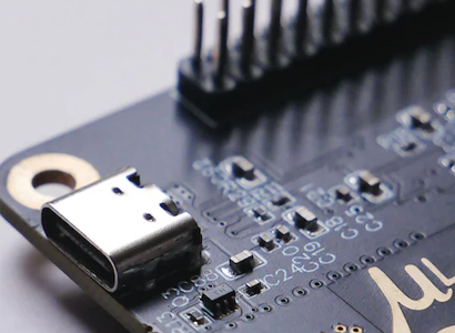
An HDI PCB is a high density interconnect PCB board using fine lines, microvias, blind vias or buried vias to achieve higher wiring density in a compact board area.

Is HDI PCB different from standard multilayer PCB?

Yes. A multilayer PCB mainly describes multiple conductive layers, while HDI PCB focuses on high-density interconnect structures such as microvias, blind vias and buried vias.

Send Your HDI PCB Files

Provide Gerber files, stack-up, material requirements, layer count and HDI structure details. PCBXINSHUN will review your HDI PCB project and provide manufacturing support.

Request HDI PCB Quote

Mainly engaged in the production of multi-layer high-precision, high-difficulty PCB, HDI, rigid-flex boards, buried blind via boards and other products

133 1645 5968

Contact Now

CASE