HDI PCB Manufacturing for Compact, High-Performance Electronics

Create more routing space for fine-pitch components with laser microvias, via-in-pad structures, and multilayer HDI stackups. XinshunPCB helps align interconnect density, materials, and impedance requirements for compact devices and high-speed electronics.

Request an HDI PCB Quote

HDI PCB specifications

Review HDI structures, microvias, and fabrication parameters for your next design. Values below are planning references; the available combination of layer count, copper weight, hole geometry, and tolerances must be confirmed by XinshunPCB during DFM review before ordering.

HDI structure & microvias

Parameter Specification
HDI structures 1+N+1, 2+N+2, 3+N+3; any-layer subject to review
Laser microvia diameter 0.1 mm (4 mil); finer features require review
Microvia capture pad Design reference: from approximately 0.25 mm
Microvia types Stacked, staggered, and skip vias
Via fill Copper-filled; resin-filled, capped, and planarized (VIPPO)
Build-up Sequential lamination; multiple build-up layers
Minimum blind / buried via Design reference: 0.1 mm within 1–18 layers
Through-hole aspect ratio Design reference: up to approximately 10:1

Lines, spacing & holes

Parameter Mass production Prototype (extended)
Minimum inner-layer clearance 3 mil 3 mil
Minimum line width 3 mil (0.075 mm) 3 mil (0.075 mm)
Minimum line space 3 mil (0.075 mm) 3 mil (0.075 mm)
Minimum mechanical hole 0.1 mm 0.1 mm
Minimum plated hole copper 25 µm 25 µm
PTH diameter tolerance ±0.076 mm (±3 mil) ±0.076 mm (±3 mil)
NPTH diameter tolerance ±0.05 mm (±2 mil) ±0.05 mm (±2 mil)
Hole position deviation ±0.05 mm (±2 mil) ±0.05 mm (±2 mil)

Layers, copper & legend

Parameter Mass production Prototype (extended)
Overall layer count — subject to review 1–24 layers 1–78 layers
Heavy copper — subject to review 4 oz (140 µm) Up to 12 oz
Minimum solder-mask bridge 0.1 mm (4 mil) 0.1 mm (4 mil)
Solder-mask colour Green, Black, Blue, White, Yellow, Red Green, Black, Blue, White, Yellow, Red
Silkscreen colour White, Yellow, Red, Black White, Yellow, Red, Black

Outline & mechanical

Parameter Mass production Prototype (extended)
Outline method Routing, V-groove, beveling, punch Routing, V-groove, beveling, punch
Outline tolerance ±0.15 mm (±6 mil) ±0.15 mm (±6 mil)
Peelable mask Top, bottom, double-sided Top, bottom, double-sided

Electrical & reliability

Parameter Mass production Prototype (extended)
Controlled impedance ±10% ±7%
Insulation resistance 1 × 10¹² Ω (normal) 1 × 10¹² Ω (normal)
Through-hole resistance — test definition to confirm < 300 Ω (normal) < 300 Ω (normal)
Thermal shock 3 × 10 seconds at 288 °C 3 × 10 seconds at 288 °C
Warp & twist ≤ 0.7% ≤ 0.7%
Electric strength > 1.3 kV/mm > 1.4 kV/mm
Flammability — material recognition to confirm 94V-0 94V-0
Test voltage 50–330 V 50–330 V

Have an HDI board to build?

Send your Gerbers, proposed stackup, and via map to XinshunPCB. Our engineers will review the build-up structure, microvia requirements, and manufacturability, then provide a quotation and DFM feedback for your project.

Request an HDI PCB Quote

Advanced HDI Processes for Dense, Reliable Interconnects

Combine microvia structures, fine-line routing, and controlled stackups to support miniaturization and high-speed performance. The final process route is reviewed against your design and qualification requirements.

Any-layer HDI

Connections between successive layers can shorten escape routes and free routing space around high-pin-count devices. Select an any-layer structure after reviewing density, layer transitions, and reliability requirements.

Any-layer interconnect

Stacked & filled microvias

Copper-filled laser microvias can be arranged in stacked or staggered patterns. Match the arrangement to the layer transitions, available pad area, and agreed qualification plan.

Copper-filled microvias

Via-in-pad (VIPPO)

Filled, capped, and planarized vias allow routing connections within component pads. Define the filling and plating requirements to support fine-pitch BGA assembly.

Filled & plated over

Sequential lamination

Successive build-up and lamination stages connect outer routing layers to the core. Review 1+N+1, 2+N+2, and more complex structures against the required routing density.

HDI build-up

Fine-line routing

Fine trace geometries help route dense component areas. Select copper thickness and the appropriate imaging and etching process; advanced mSAP requirements need a separate process review.

Fine-pitch routing

High-speed & impedance

Coordinate dielectric materials, trace geometry, and reference planes across the HDI stackup. Define impedance targets and test coupons before releasing the design.

Signal integrity

Quality Standards for HDI PCB Projects

Define the applicable design, board acceptance, assembly, and quality requirements before production. XinshunPCB reviews the required standard revision, acceptance class, test plan, and certification scope for each HDI project.

IPC-2226

HDI design requirements

IPC-6016

HDI qualification requirements

IPC-6012

Rigid-board performance

IPC-A-600

Bare-board acceptance

IPC-A-610

Assembly acceptance criteria

ISO 9001

Quality management

UL / 94V-0

Confirm material recognition

RoHS / REACH

Material compliance requirements

ISO 13485

Medical quality requirements

IATF / AS9100

Confirm project-specific scope

Related Solutions

Explore PCB and assembly solutions for compact connected devices, medical electronics, and other systems that benefit from high-density interconnects.

Industrial & Power Electronics

Industrial & Power Electronics

Engineered to withstand massive electrical currents, thermal stress, and continuous mechanical vibration. XinshunPCB delivers IPC Class 3 heavy copper boards, high-thermal metal-core solutions, and turnkey SMT assemblies for grid-scale energy storage, industrial robotics, motor drives, and solar inverters.

Explore Solution
Telecommunications & IoT

Telecommunications & IoT

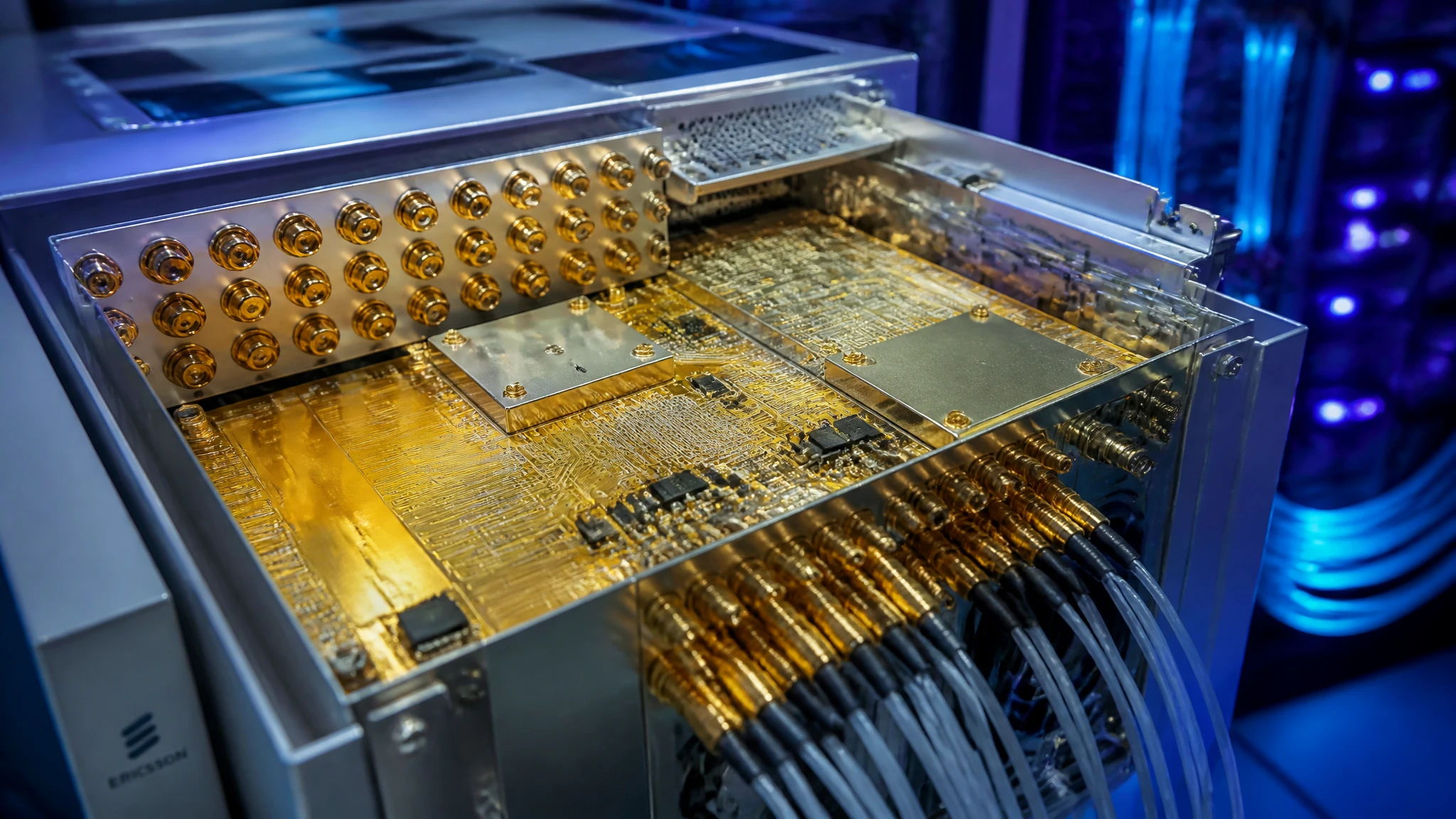
From wireless gateways and connected sensors to networking equipment, XinshunPCB supports custom PCB fabrication and assembly for communication hardware. Align materials, stackups, compact layouts, and production testing with your application, from initial prototypes to repeat production.

Explore Solution
Medical Equipment

Medical Equipment

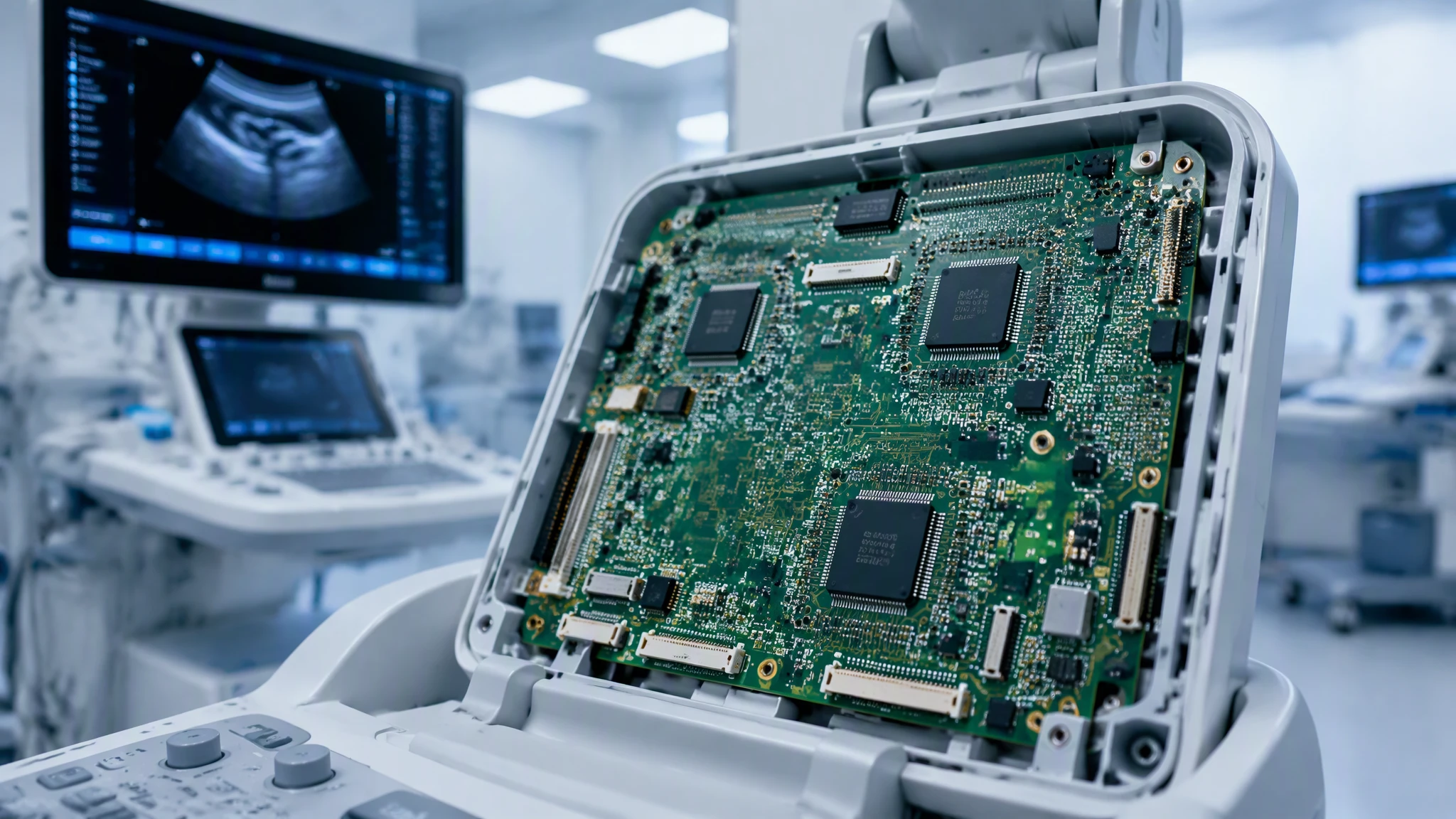
From patient monitoring and diagnostic instruments to medical imaging systems, XinshunPCB provides custom PCB fabrication and PCBA assembly for healthcare equipment. We help you align board materials, circuit layouts, and assembly requirements with your application, supporting development from initial prototypes to production.

Explore Solution
Automotive Electronic

Automotive Electronic

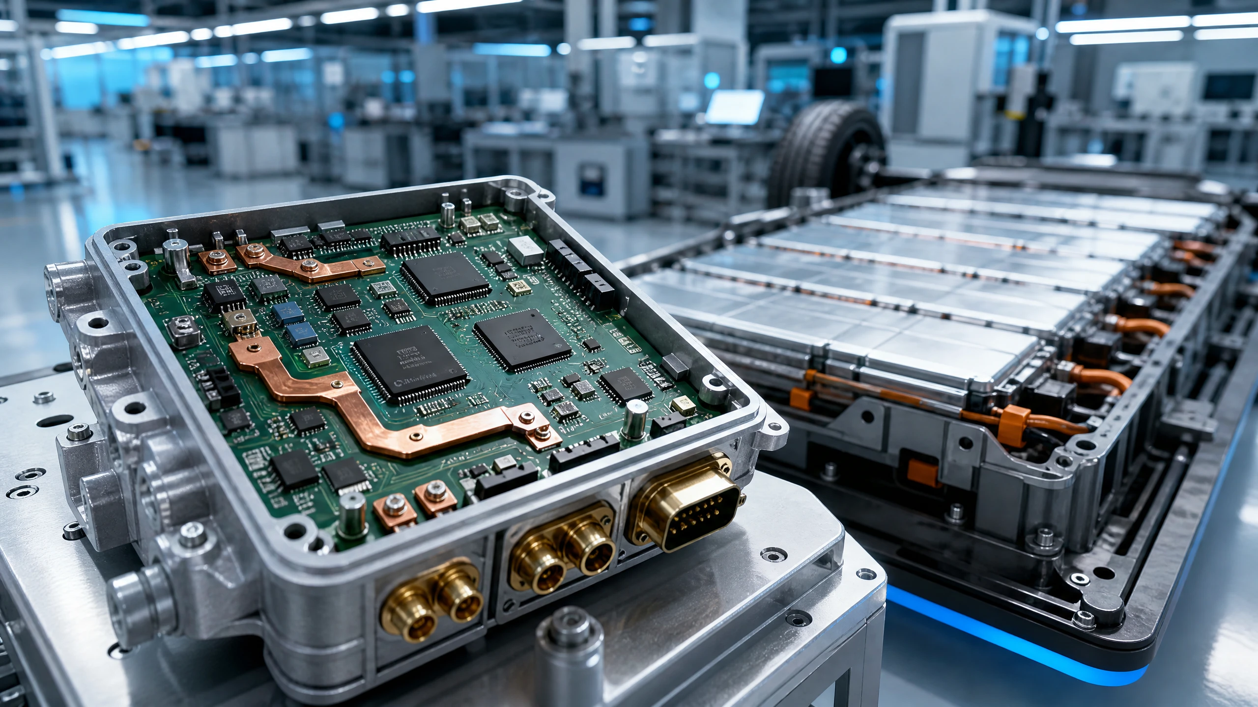
Engineered to withstand extreme mechanical shock, high-voltage switching surges, and thermal cycling from –40°C to +150°C. XinshunPCB delivers IATF 16949-aligned, IPC-A-610 Class 3 turnkey PCB fabrication and SMT assembly for electric vehicle (EV) powertrains, ADAS sensing, high-voltage BMS, and under-hood body control modules.

Explore Solution

HDI PCB Design & Manufacturing FAQ

Find practical answers about HDI stackups, microvias, via-in-pad, materials, testing, and the files needed for a manufacturing review.

Q1 What is an HDI PCB and when should it be used? +
An HDI PCB uses fine routing features and small interlayer connections, such as laser microvias, to increase routing density. It is useful when fine-pitch BGAs, high-pin-count devices, or limited board space make conventional routing difficult. The appropriate structure depends on component pitch, signal paths, layer count, and reliability requirements.
Q2 How should I choose an HDI build-up and microvia structure? +
Start with the required component escape routing and layer transitions. A 1+N+1 structure uses one build-up layer on each side of a core, while 2+N+2 adds further build-up layers. Staggered microvias need lateral routing space; stacked microvias place connections above one another and require a suitable filling and qualification process. Review the stackup, via map, and reliability criteria together before fabrication.
Q3 When is via-in-pad (VIPPO) needed for an HDI PCB? +
Via-in-pad can provide an escape route within a component land where fine-pitch routing leaves little space for a separate via. The drawing should identify the vias that need filling, capping, and planarization, along with the required surface finish. An open via in a solder pad can draw solder away from the joint, so the agreed via treatment must be compatible with the assembly process.
Q4 How are materials and controlled impedance selected for HDI PCBs? +
Select materials by considering signal frequency, loss budget, operating temperature, lamination cycles, and reliability needs. Impedance depends on the dielectric thickness and properties, copper thickness, trace geometry, and reference planes. Provide the impedance targets, tolerances, and signal-layer assignments so the stackup and verification coupons can be reviewed before production.
Q5 What inspection and testing should be specified for an HDI PCB? +
Define the acceptance class and test plan in the fabrication documentation. Depending on the design, inspection may include AOI, continuity and isolation testing, microsections of plated or filled vias, X-ray inspection, and impedance measurements. Thermal stress or other reliability tests should use agreed coupons, sampling, and acceptance criteria relevant to the HDI construction.
Q6 What files are needed for an HDI PCB quotation and DFM review? +
Provide Gerber or ODB++ data, drill files, the proposed stackup, fabrication notes, and order quantities. Include a via map identifying laser, blind, buried, stacked, and via-in-pad connections; specify material, copper weight, impedance, surface finish, and test requirements. For assembly, add the BOM, placement files, and assembly drawings. XinshunPCB can then review manufacturability and quote the agreed build.


Get Your Custom PCB & PCBA Quote in 24 Hours

Have a new project or custom PCB requirements? Simply fill in your project details below. XinshunPCB’s FAE engineering team will analyze your specifications and deliver a detailed formal quotation along with free engineering advice within 2–24 hours.

24-Hour Fast Turnaround

Detailed formal quote & lead time provided within 2-24 hours.

100% Privacy & NDA Protection

Your contact info and project specs are kept strictly confidential.

Free Engineering Consultation

Experienced FAE support to help optimize your specifications.

Email WhatsApp