

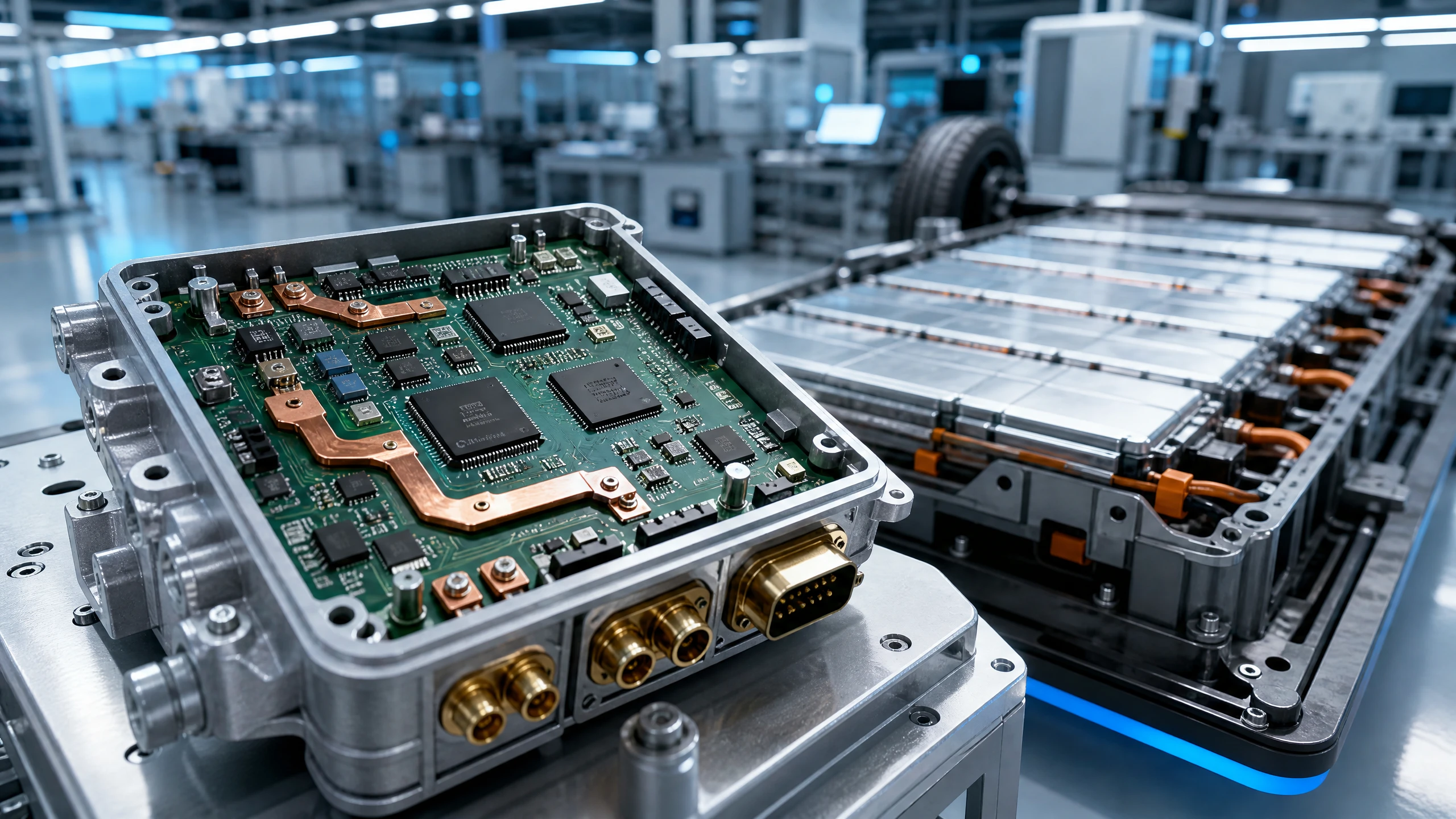
Automotive Electronic
Automotive PCB and PCBA solutions designed for vibration, thermal cycling, and long-life reliability.
Explore Automotive Electronic Solutions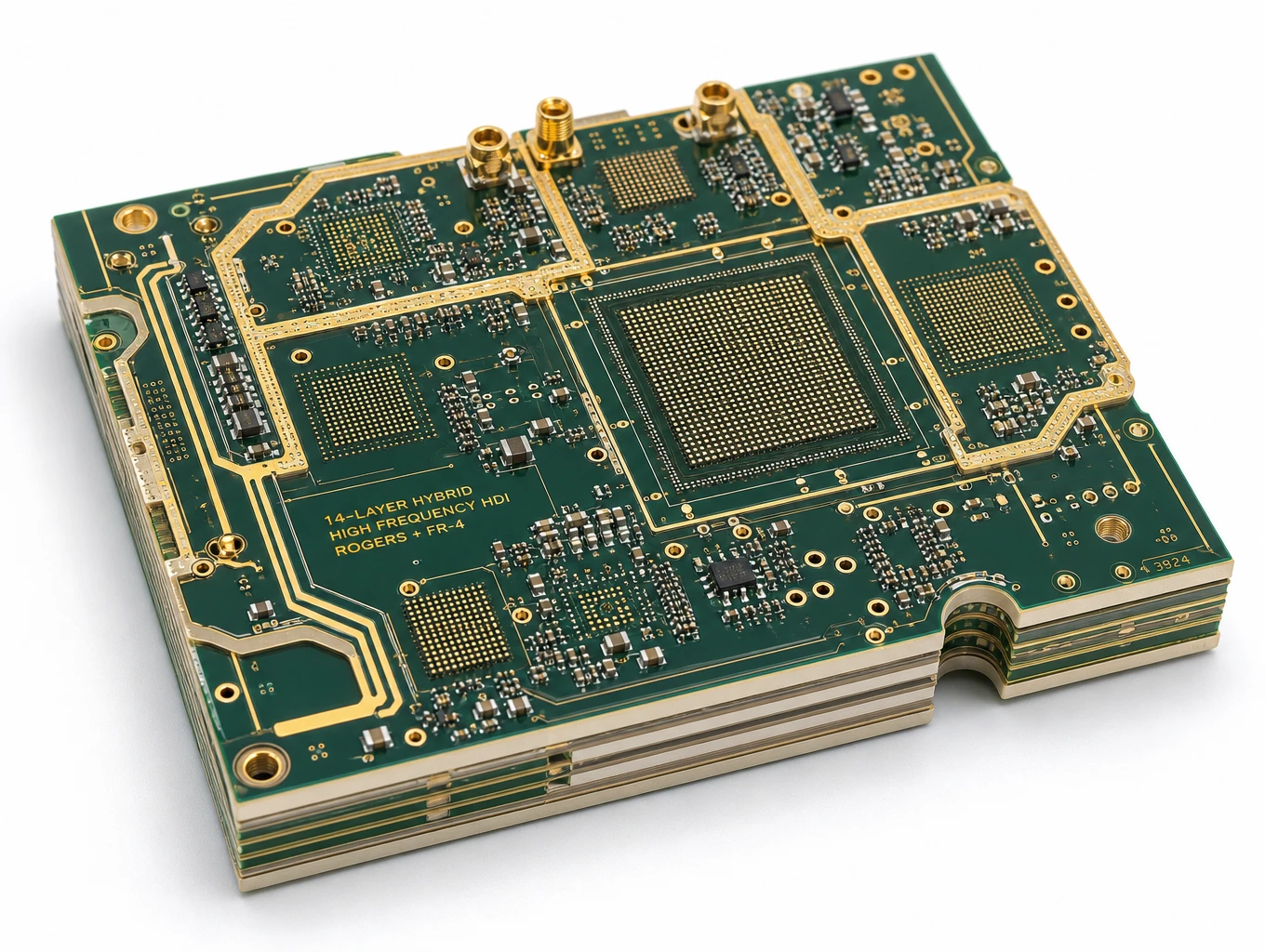
Built for millimeter-wave communications and high-frequency radar modules, this 14-layer hybrid HDI board bonds low-loss Rogers ceramic hydrocarbon laminates with High-TG FR-4 cores. Featuring laser-drilled microvias down to RF reference planes and strict ±5% impedance tolerances, it delivers clean transmission lines with minimal phase noise and dielectric insertion loss.
From standard 1+N+1 microvia builds to complex Any-Layer HDI (ELIC) and ultra-fine-pitch architectures, XinshunPCB combines German UV/CO2 laser micro-machining, automated VIPPO copper planarization, and sub-mil trace etching to maximize routing density without compromising high-frequency signal integrity.
Engineered for compact wearables, automotive ADAS sensors, and high-tier medical instruments requiring maximum components per square centimeter. Utilizing German multi-beam CO2 and UV laser systems, we achieve microvia diameters down to 50–75 µm with stacked and staggered via structures up to Any-Layer HDI (ELIC, 10+ layers). Automated chemical desmear and electroplated copper filling produce solid, void-free via barrels that withstand severe thermal expansion cycles.

Eliminates routing bottlenecks and solder bridging beneath dense micro-BGA packages. We deploy Via-in-Pad Plated Over (VIPPO / POFV) processes featuring automated resin plugging, ceramic planarization, and electroplated copper capping to maintain pad coplanarity within < 15 µm. Combined with fine line width and spacing down to 40 µm / 40 µm (1.6 mil), designers can place microvias directly inside 0.30–0.35 mm pitch component pads without solder loss during reflow.

Built to eliminate signal attenuation and reflection in high-speed digital lines and 5G RF transceivers. We manufacture hybrid stackups combining Rogers, Isola, or Panasonic Megtron low-loss laminates with High-TG FR-4 cores. Using Polar SI9000 field simulation tools and automated chemical differential etching, we hold single-ended and differential impedance tolerances strictly to ±5%, verified batch-by-batch via coupon-level Time-Domain Reflectometry (TDR) testing.


Pushing the boundaries of spatial density, microvia miniaturization, and high-speed signal routing. From 1+N+1 to Any-Layer ELIC architectures, German UV/CO2 laser micro-drilling, and planarized VIPPO copper capping, our automated in-house manufacturing keeps your high-density interconnect designs manufacturable, scalable, and IPC-6012 Class 3 compliant.
Operating environments leave zero room for hardware failure. Built upon our 6 core product categories, XinshunPCB delivers specialized circuit fabrication, IPC Class 3 assembly, and thermal management solutions customized for 4 high-growth global industries.
Automotive PCB and PCBA solutions designed for vibration, thermal cycling, and long-life reliability.
Explore Automotive Electronic SolutionsFind quick answers about HDI stackup configurations, laser microvia drilling, VIPPO planarization, fine-pitch BGA design rules, and IPC Class 3 quality inspection.
All HDI boards are manufactured and verified to IPC-A-600 Class 2 and Class 3 standards. The inspection gate includes:
100% Electrical Netlist Testing: High-density double-sided flying probe testing checking continuity and isolation down to low-resistance thresholds.
Automated Optical Inspection (AOI): Multi-spectral AOI inspecting inner and outer fine lines, spacing, and microvia annular rings against customer Gerber/ODB++ datasets.
High-Resolution 3D X-Ray Inspection: Verifying layer-to-layer microvia alignment, registration, and stacked via barrel fill integrity.
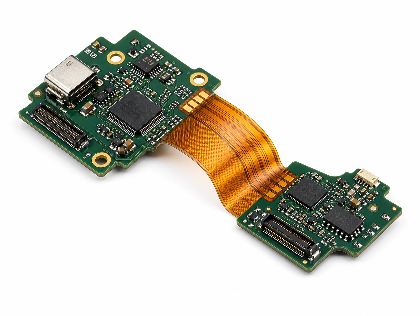
Looking for flexible 3D spatial integration, extreme power thermal management, or full box-build electronic assembly? Explore XinshunPCB's complementary product categories engineered to support your complete hardware lifecycle from bare board fabrication to full turnkey assembly.
Have a new project or custom PCB requirements? Simply fill in your project details below. XINSHUNPCB's FAE engineering team will analyze your specifications and deliver a detailed formal quotation along with free engineering advice within 2-24 hours.

Detailed formal quote & lead time provided within 2-24 hours.

Your contact info and project specs are kept strictly confidential.

Experienced FAE support to help optimize your specifications.
Need a reliable manufacturing partner for your next project? Our global support team is standing by.
Trusted by global integrators for PCB manufacturing, enterprise hardware, and high-reliability deployment solutions.