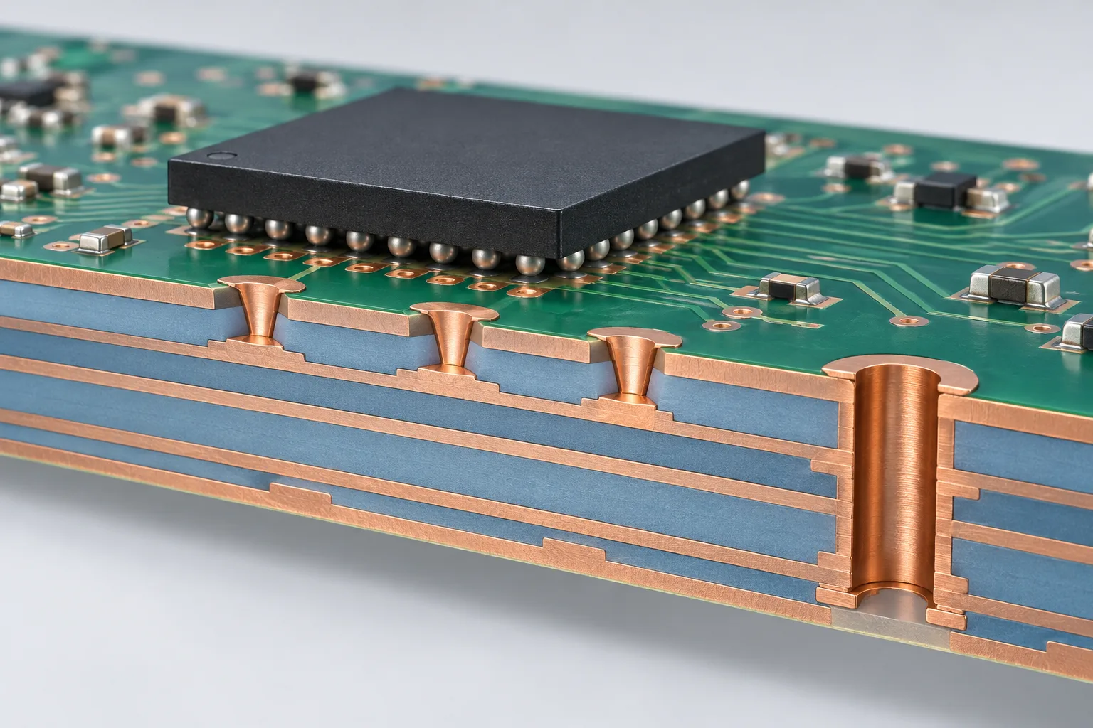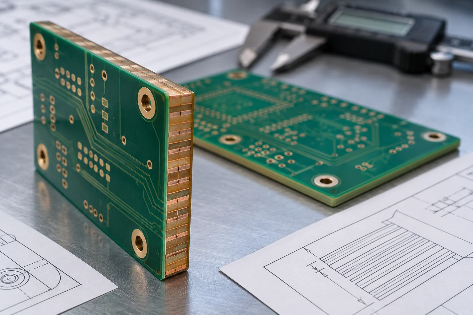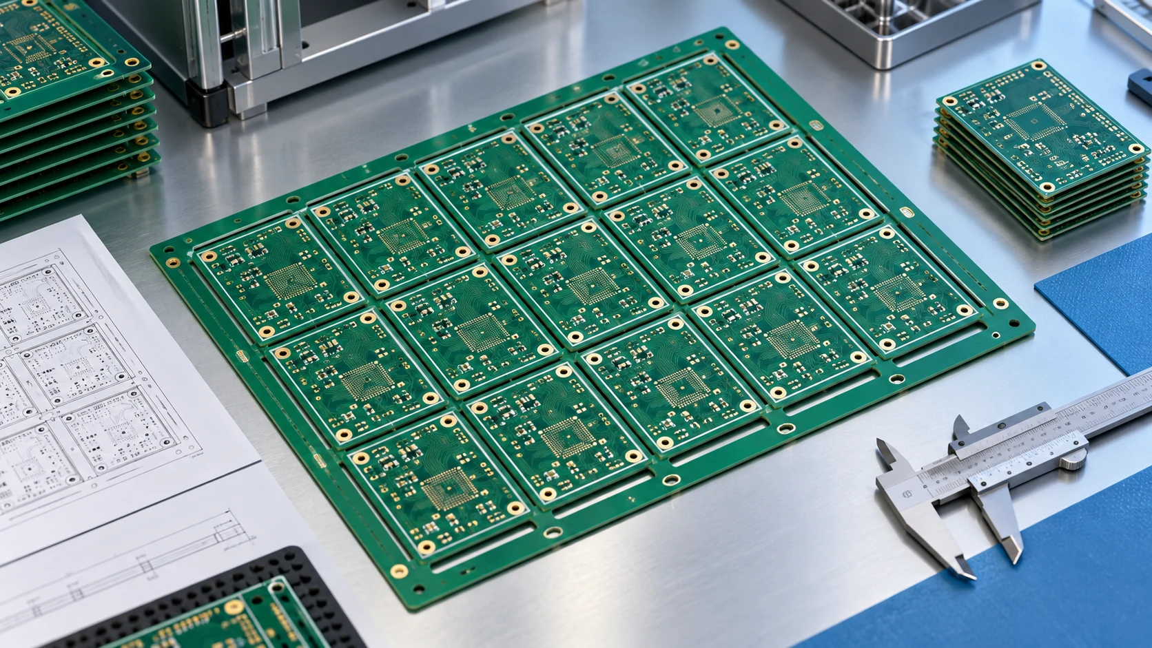

Choose the Microvia Path Before Freezing the HDI Layout
Stacked vs staggered microvias is a choice about where successive layer connections sit. Stacked microvias align vertically to conserve routing area. Staggered microvias use offset positions joined by copper on an intermediate layer. Choose the arrangement by reviewing the escape routing, approved fabrication process and reliability evidence together.
For buyers sourcing custom HDI PCB fabrication, a drawing marked “stacked vias” is only the start of the specification. The supplier needs the exact layer spans, pad geometry and treatment. Your acceptance plan must also identify which construction is being evaluated.
The broader HDI PCB design guidelines explain 1+N+1, 2+N+2 and any-layer build-ups. This comparison focuses on the arrangement of successive microvias within those constructions, helping designers and procurement teams resolve a specific routing and manufacturing decision.
- Identify which layer transitions need vertical alignment and which can be offset.
- Approve the via geometry, fill and manufacturing sequence with the fabricator.
- Compare reliability evidence and quotation scope for the actual construction.
What Is the Physical Difference Between Stacked and Staggered Microvias?
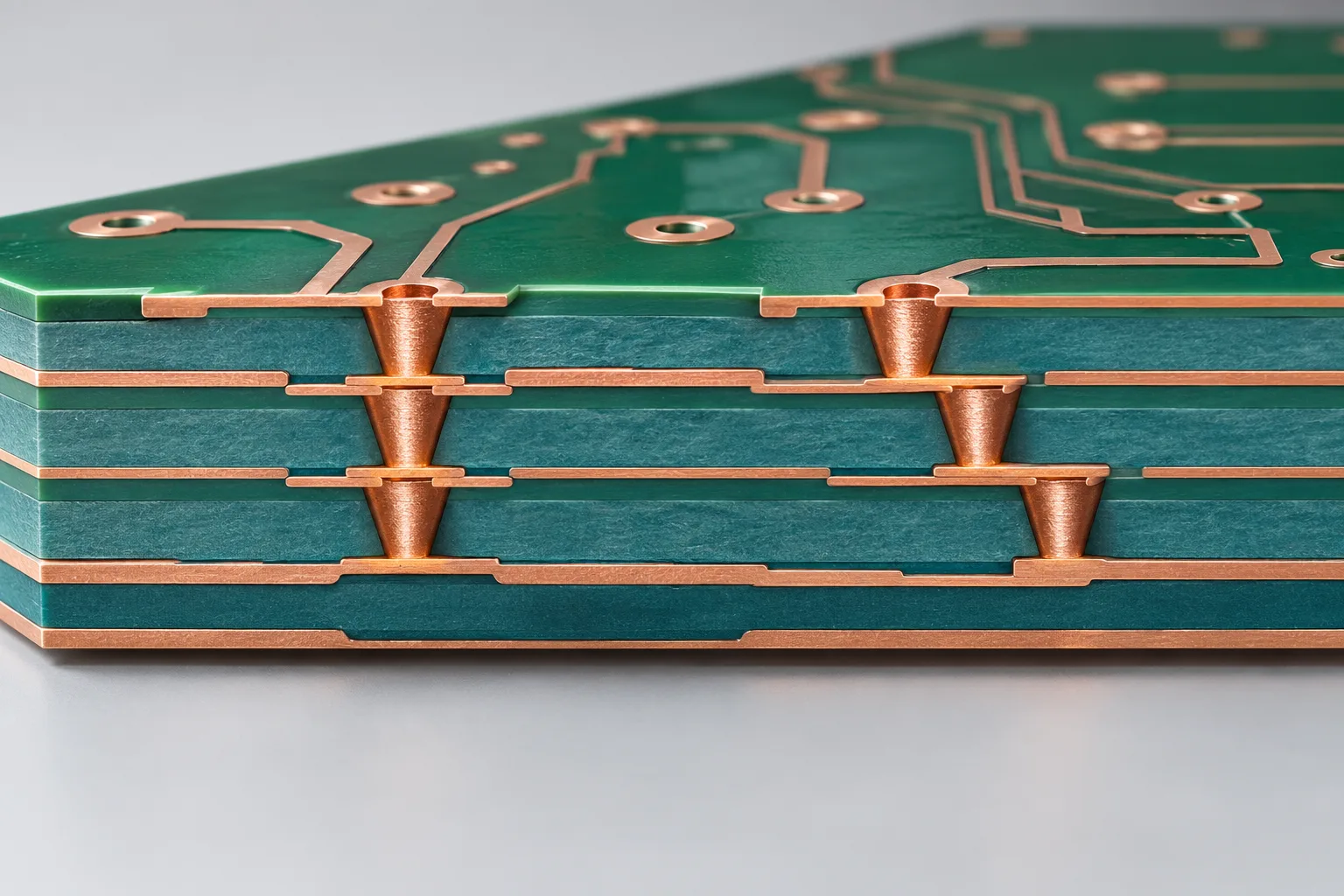
A stacked path places successive microvias on a common vertical axis. A staggered path moves the next microvia sideways and connects the two locations with copper on their shared layer. Both arrangements can join the same starting and ending layers, while occupying different space on the intermediate layer.
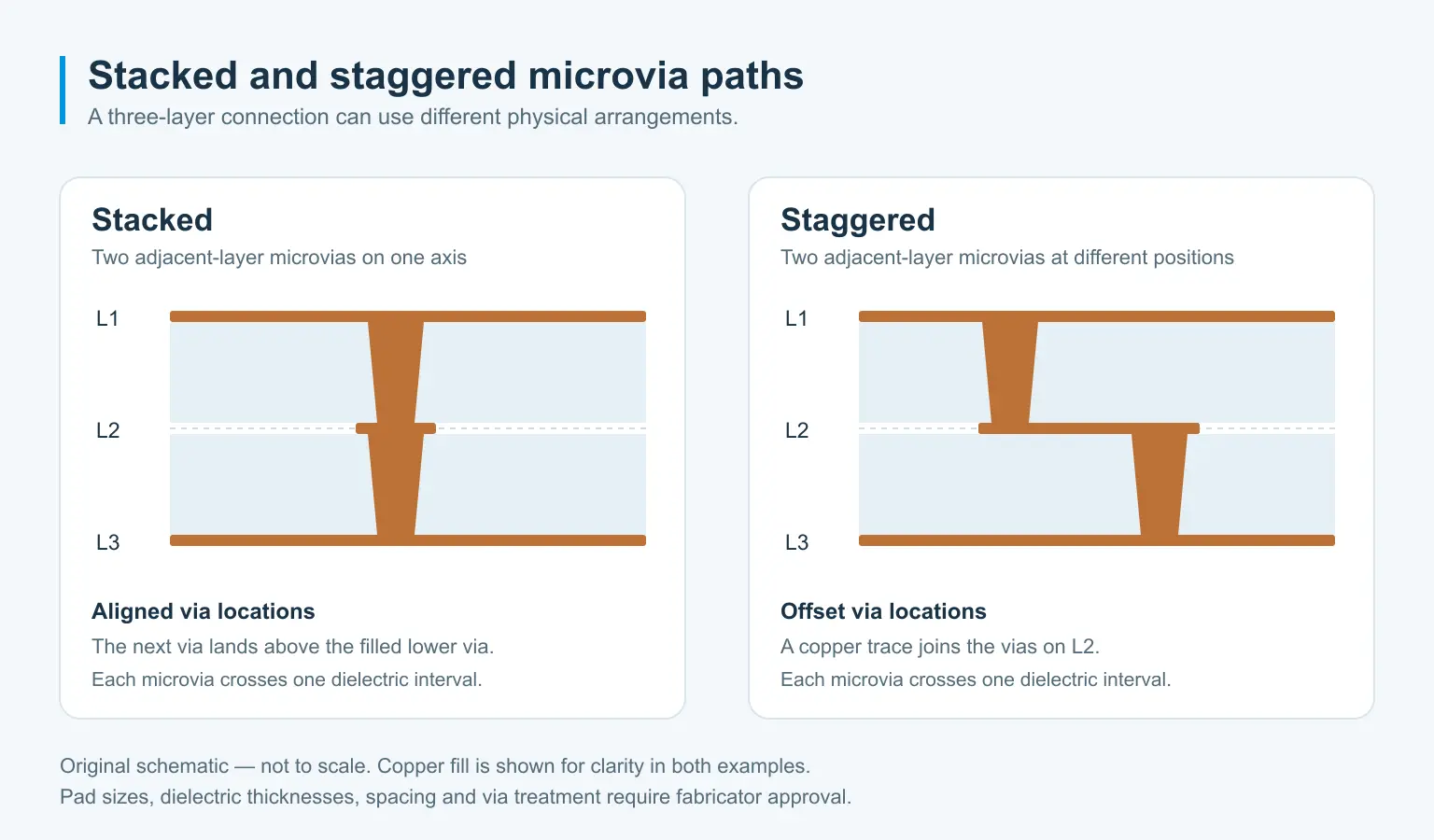
In the three-layer example above, one microvia connects L1 to L2 and another connects L2 to L3. The staggered example includes a short connection along L2. The stacked example needs an approved landing surface for the upper microvia above the lower connection. Neither drawing represents one laser hole through all three copper layers.
Altium’s overview of HDI interconnect structures describes the internal copper connection used by staggered vias and recommends agreeing stacked-via geometry with the fabricator. Number every layer in the via map. Do not rely on a plan view where two features appear aligned but their actual spans are unclear.
Compare the Tradeoffs Against Your Routing Constraints
Stacking is useful when the intermediate layer cannot accommodate the lateral move. Staggering is worth evaluating when space exists for that move and its connecting trace. The right comparison uses the actual component escape, not an isolated picture of a via or a generic rule based only on BGA pitch.
| Review item | Stacked arrangement | Staggered arrangement |
|---|---|---|
| Routing footprint | Concentrates successive transitions in one local position | Needs lateral room for the offset and copper connection |
| Intermediate layer | An aligned landing must be compatible with the approved fill and process | The connecting trace and both pads occupy routing space |
| Fabrication definition | Specify every microvia span, fill requirement and any underlying buried via | Specify spans, offset, connection width and whether filling is required |
| Reliability review | Examine the actual interfaces and construction-specific evidence | Assess the complete geometry and process; the offset is not a qualification result |
| Signal path | A compact transition still needs reference and impedance review | The additional lateral segment belongs in the channel review |
| Price comparison | Quote the approved process and verification scope | Compare on the same board, materials and acceptance basis |
Consider an escape path that reaches L3 from L1. If the L2 routing area can accommodate a connecting trace and its clearances, ask the fabricator to assess a staggered option. If that area is already occupied, evaluate whether stacking solves the restriction without introducing an unqualified construction. This is a design-review example, not a tested production result.
A board may use different arrangements in different regions. Mark those regions and via families clearly so the fabricator can review the combined route. A local space saving does not establish that the whole board needs an any-layer build, and a staggered connection does not automatically reduce its build-up stages.
Review Filling, Landing Surfaces and the Manufacturing Sequence
An upper microvia must land on a surface suitable for the approved process. For a stacked structure, the treatment of the underlying microvia matters directly to that landing. Agree the fill, surface condition and tolerances with the fabricator before releasing the artwork. Do not leave the supplier to infer them from pad overlap.
Würth Elektronik’s HDI design-rules poster distinguishes standard and copper-filled microvias, stacked and staggered arrangements, and filled-and-capped via constructions. Its dimensions apply to its documented processes. Use the document to understand what must be specified, rather than transferring its dimensions to an unrelated XinshunPCB build.
XinshunPCB’s HDI manufacturing capability page lists stacked, staggered and skip-via options for engineering review. Confirm the permissible combination for your dielectric intervals, pad geometry, copper and materials. Also identify any microvia positioned over a mechanically drilled buried via, because that underlying structure is part of the review.
Ask the supplier to return a numbered construction and process sequence. It should make clear which layer pair is drilled at each relevant stage and which underlying vias receive additional treatment. A two-stage microvia path drawn in CAD does not, by itself, specify the number of lamination operations or the production acceptance requirements.
For the pad treatment itself, use the via-in-pad filling and copper-capping guide to define the finished solderable surface, inspection evidence and files to include in your manufacturing RFQ.
How Should Microvia Reliability Be Evaluated?
Evaluate the geometry and manufacturing process as a qualified construction. Staggering can avoid a direct stack of successive microvia interfaces, but it does not guarantee service life. Likewise, a stacked structure should be assessed against relevant process capability and test evidence rather than accepted or rejected solely by its name.
In its March 2019 warning on microvia reliability, IPC described failures that became apparent after traditional bare-board acceptance, including after reflow and in service. It highlighted weak microvia interfaces and the limitations of relying on conventional microsection inspection alone. This historical warning supports a focused verification plan; it is not a statement that every stacked structure fails.
Ansys’ discussion of microvia fatigue analysis describes a general reliability advantage for staggered arrangements and explains the role of thermal-expansion mismatch and manufacturing defects. It also relates interfacial separation to the reflow process. Such a trend cannot be used as a numerical life prediction for an untested board or as approval of a particular supplier.
For the proposed build, agree representative test structures, conditioning, electrical monitoring, sample scope and acceptance criteria. Ask whether the evidence covers the relevant via arrangement, materials and manufacturing route. Keep prototype qualification distinct from routine lot acceptance, and define which changes require a new review.
When a supplier offers an alternative, record both its construction and its supporting evidence. A microsection image can help describe a structure, while a room-temperature continuity result describes connectivity under those test conditions. Decide what additional evidence is appropriate for the application before the order is placed.
Include Signal References and Cost in the Same Decision
Review the full signal path and quotation scope after choosing an arrangement. A shorter geometric path is not enough to establish channel performance, and an offset path is not automatically less expensive. Compare complete constructions with the same electrical targets, materials, quantities and agreed inspection requirements.
Check the reference path through the layer change
Use the PCB stackup review checklist to identify signal layers and reference planes. Include the intermediate trace in a staggered connection, nearby copper clearances and the return-path arrangement. Have the electrical design owner assess critical transitions using the modelling and verification appropriate to the interface.
Compare quotations after assumptions are closed
The PCB manufacturing cost guide explains why board construction and process choices influence a quotation. For this comparison, ask suppliers to identify the cost of the proposed via treatment, process route and test scope. Avoid a fixed savings claim based only on replacing “stacked” with “staggered” in the drawing.
Keep the outline and connected nets consistent while reviewing alternatives. If a proposal changes the layer count, material, routing area or acceptance plan, document those changes separately. Procurement can then distinguish a process substitution from a change to the board being purchased.
Put the Via Arrangement into a Reviewable B2B RFQ
A useful RFQ combines the via map with the stackup and an explicit list of open questions. Give each via family a clear identifier. Ask the supplier to return exceptions in writing so the design owner can approve any change before fabrication, rather than discovering it in a later drawing revision.
| RFQ detail | What to define | What to ask the supplier |
|---|---|---|
| Layer connections | Start and end layer for every microvia; identification of any underlying core via | Does the proposed process support these exact transitions? |
| Geometry | Dielectric interval, hole and pad definitions, offset or alignment, tolerances | Which production values and registration allowances are approved? |
| Via treatment | Copper fill or other agreed treatment, cap/planarization locations and surface needs | Which features are included in the quotation? |
| Electrical intent | Affected nets, reference planes and critical-interface requirements | Which construction details must return to the electrical designer? |
| Verification | Representative coupons, conditioning, monitoring, sampling and acceptance scope | Does the evidence represent this construction? |
| Commercial release | Revision, quantities, required records and prototype-to-production plan | What changes trigger renewed approval? |
Start with the PCB quotation file checklist and add the arrangement-specific information above. Send the controlled fabrication data and via schedule together. Keep any proposed alternative in an exception list until both the design owner and the supplier approve it.
For example, if a fabricator proposes moving an L2-to-L3 microvia to avoid a stack, request the new pad location, connecting trace and required clearances. Return that detail to layout and electrical review. Updating only the word “staggered” in a fabrication note leaves the actual change undefined.
Request a Stacked or Staggered Microvia Manufacturing Review
Choose the arrangement after the routing need, fabrication definition and verification evidence agree. Keep the approved via map with the released stackup. If the design, material system or process route changes, assess whether the earlier approval and evidence still apply before ordering the next revision.
XinshunPCB can review the submitted HDI construction and quote an agreed manufacturing scope. Request an HDI microvia construction review with your stackup, via schedule, dense-component escape detail and quantities. Identify the locations where stacking is required and where an offset alternative may be considered.
Stacked and Staggered Microvia FAQs
Practical answers about choosing, specifying and evaluating HDI microvia arrangements.
HDI PCB Construction Examples for Your Review
Use these construction examples to discuss your own via map, materials and acceptance requirements. The final build is confirmed by project review.