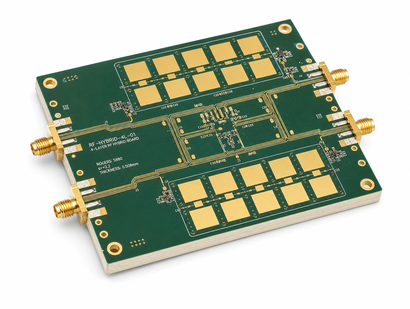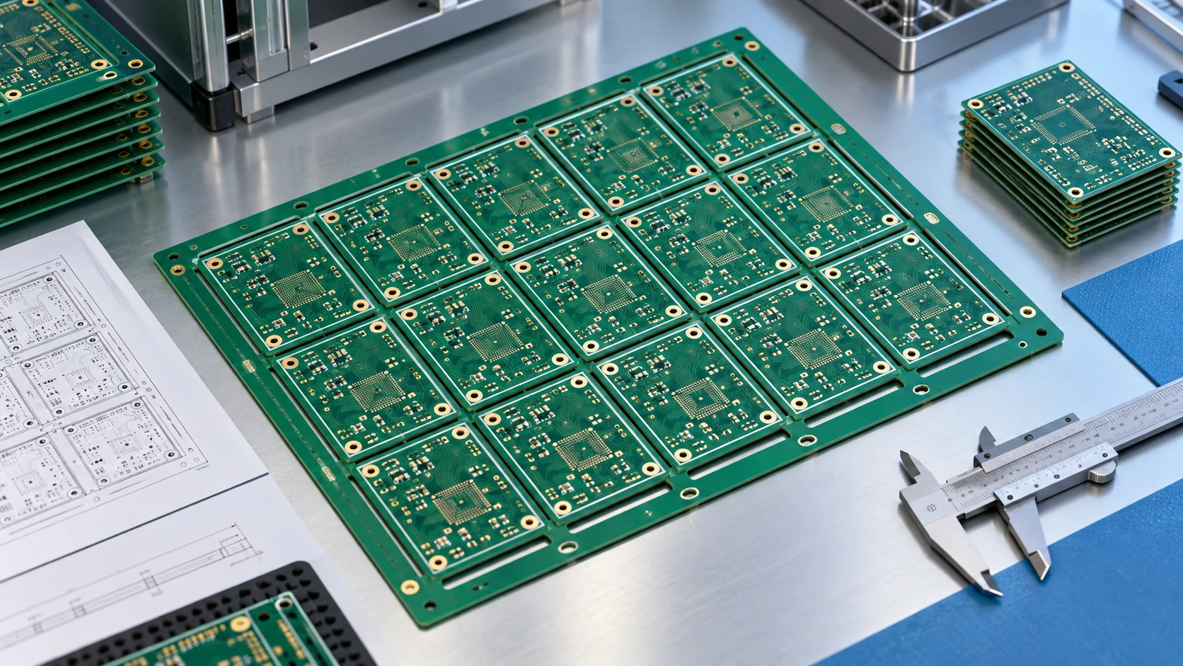

Confirm the Stackup Before Routing a Multilayer PCB
This PCB stackup design guide explains what OEM engineering and purchasing teams should agree with a fabricator before releasing a multilayer rigid board. A stackup defines the order of copper and dielectric layers, their materials and thicknesses, and the construction used for reference planes and controlled-impedance routing. Layer count alone does not define a manufacturable board.
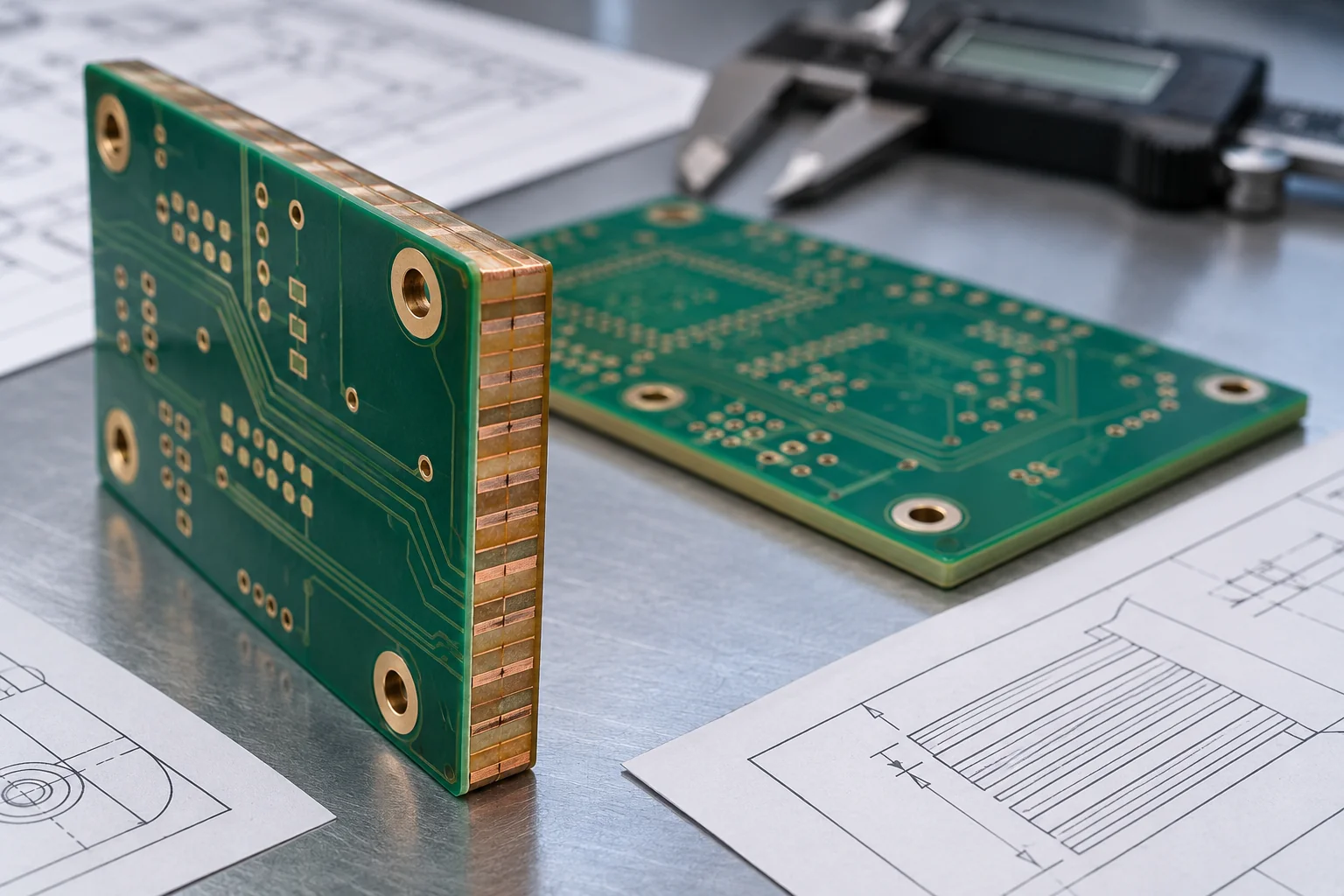
For a new design, request a proposed construction early, review it against electrical and mechanical requirements, and carry the approved version into the fabrication package. Changes after routing can affect trace geometry, via construction, finished thickness, cost and qualification. The goal is a clearly controlled design that the chosen factory can repeat.
Our rigid PCB manufacturing services are the starting point for reviewing the board family and application. Use this guide for construction decisions; the PCB manufacturing cost guide explains how material, layer count and process choices affect the commercial quotation.
Start with Electrical, Mechanical and Production Requirements
Collect requirements before selecting a familiar four-layer or six-layer template. List the important interfaces, routing density, reference-plane needs, power distribution, connector constraints, finished board thickness and assembly conditions. Evaluate critical signals using their timing and edge characteristics, not just a clock-frequency label.
- Electrical: target single-ended or differential impedance where required, relevant signal layers, reference planes, isolation needs and the basis for any loss requirement.
- Mechanical: finished thickness and tolerance, connector engagement, mounting envelope, stiff regions and flatness requirements.
- Manufacturing: achievable conductor geometry, copper distribution, hole diameters and spans, lamination sequence and inspection requirements.
- Commercial: prototype and production quantities, approved material alternatives, delivery assumptions and construction-change approval.
Keep mandatory requirements separate from preferences. A material brand required by qualification has a different status from a suggested grade that may be substituted after review. Tell the supplier which dimensions or materials can change and who may approve the change. This makes an alternative construction reviewable rather than silently different.
Assign Signal Layers and Reference Planes
Give each important routing layer a deliberate reference-plane relationship. A nearby, continuous reference helps make routing geometry and return-current behavior predictable. Plane splits, voids and transitions require review, especially when a signal changes layers or crosses a discontinuity. A layer label cannot establish that the actual copper beneath a route is continuous.
The sequences below illustrate planning choices only. They omit dielectric thicknesses, copper weights and via details, so they are not fabrication-ready stackups or impedance guarantees.
| Example | Illustrative top-to-bottom layer functions | What still needs review |
|---|---|---|
| 4 copper layers | Signal / Ground / Ground / Signal | Power distribution through suitable pours or routing, signal reference continuity and dielectric spacing |
| 6 copper layers | Signal / Ground / Signal / Signal / Ground / Signal | Coupling between central routing layers, routing direction, dielectric spacing and power-distribution allocation |
| Higher layer count | Allocate additional signal, ground and power layers to the actual routing and power needs | Plane continuity, available material builds, via spans, thickness and cost |
Symmetry of physical construction and good electrical layer allocation are related but different checks. A symmetrical sequence still needs an assessment of where signals run and how they transition. Altium’s layer-stack documentation treats copper balancing, stack symmetry and via design as considerations alongside layer definition. Review these in the board model, then ask the fabricator to confirm the build.
Specify Core, Prepreg and Material Properties
A core is a cured dielectric laminate, commonly copper-clad. Prepreg is resin-impregnated reinforcement used to bond parts of the multilayer construction during pressing. The required finished dielectric separation must be agreed for the pressed stack, not inferred from an unpressed sheet measurement.
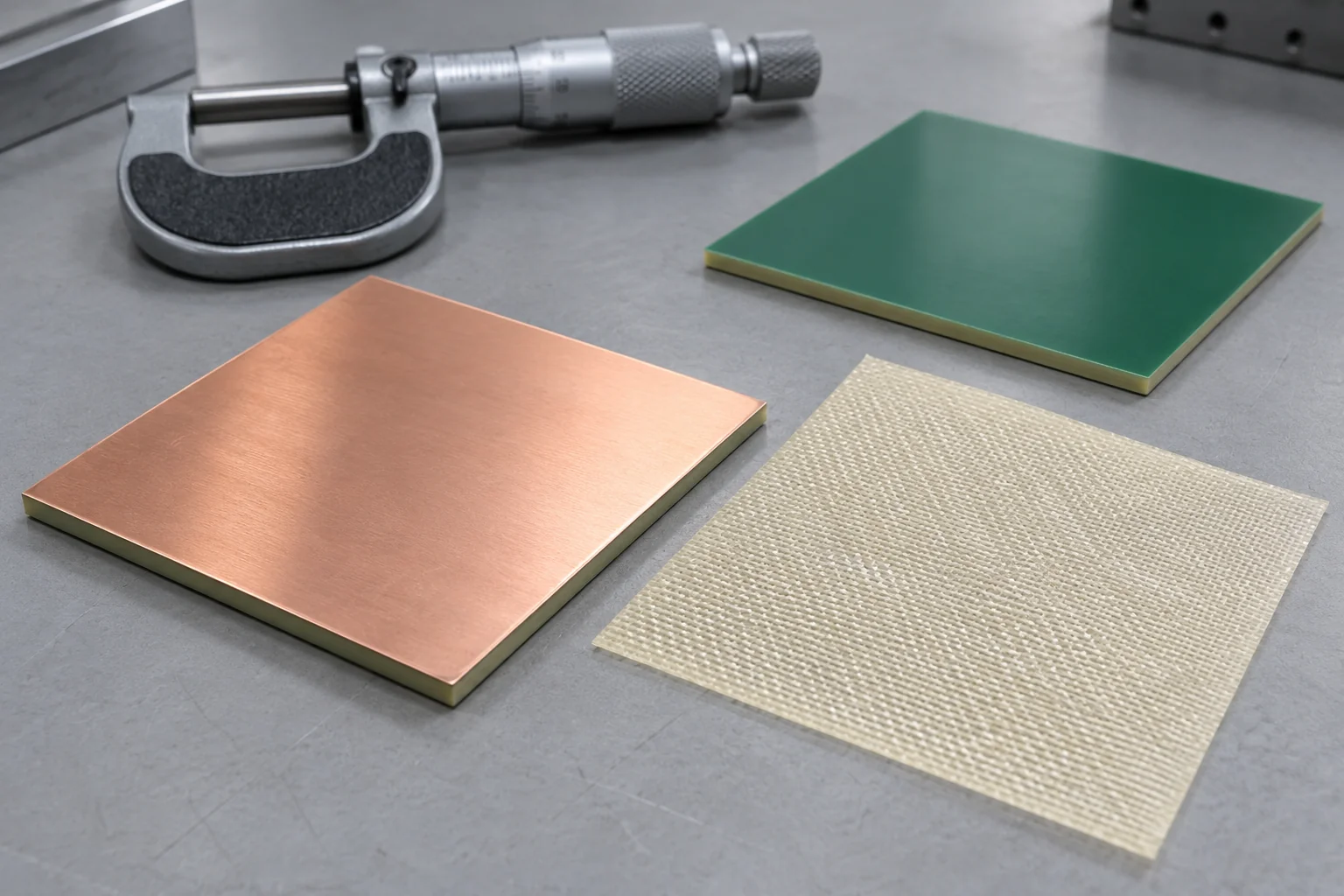
Specify the laminate family or grade, relevant thermal and electrical requirements, and permitted substitutions. “FR-4” identifies a broad material category, not a single dielectric constant or loss value. For impedance and loss-sensitive designs, agree the material data and frequency basis used by the designer and manufacturer.
Isola’s FR408HR material and construction data publishes Dk and Df at different frequencies and for different glass styles and resin contents. This illustrates why a generic material name is insufficient for every calculation. It is an example of manufacturer data, not a claim that this grade is stocked or required for your XinshunPCB project.
Ask the supplier to identify proposed cores, prepreg constructions and pressed dielectric targets. Available constructions, resin flow, copper pattern density and process controls can influence the final build. Do not approve a substitution solely because its Tg looks similar; the relevant electrical, thermal, mechanical and qualification requirements must also be considered.
Agree Controlled Impedance and Finished Copper
For every controlled-impedance structure, state the target, tolerance, routing layer and reference planes. Identify whether it is single-ended, differential or another specified structure. Include the trace width, differential gap where relevant, nearby copper clearance and solder-mask assumptions used in the calculation.
Altium’s controlled-impedance routing guidance connects layer-stack material settings and impedance profiles to routing constraints. A calculator result needs the correct construction inputs; a default library value is not supplier approval.
Distinguish starting copper foil from finished conductor copper. Outer-layer plating and etching affect the geometry, and inner and outer layers may have different specified copper. Ask whether proposed width adjustments remain within your design constraints. Document the approved values instead of allowing an unspecified change to every critical trace.
Agree how the build will be checked: coupon structures, measurement method, reporting, acceptance limits and treatment of exceptions. A coupon is a defined production check; it does not validate every routed interconnect or replace system-level signal-integrity review. The rigid PCB manufacturing capabilities page provides the relevant company process context. Have the project team confirm which limits and verification steps apply to the actual construction.
Review Copper Balance, Vias and Lamination Together
Review dielectric and copper thicknesses around the board’s center together with the distribution of actual copper patterns. A physically balanced build is a useful starting point for managing deformation, but layer symmetry alone cannot guarantee final flatness. Large copper-density differences, heavy copper regions and unusual shapes need specific manufacturing review.
Define which layers each hole connects, whether it is a through hole, blind via or buried via, and whether sequential lamination, filling or back drilling is required. The stackup controls via length and possible construction sequences. Hole diameter and finished thickness must be reviewed together rather than as independent limits.
Use extra process steps only where the design requires them. Adding layers can simplify routing or reference allocation, but can also change thickness, material requirements and fabrication complexity. A lower layer count can require tighter routing or a more specialized via build. Compare feasible alternatives against electrical requirements and total manufacturing scope rather than choosing the cheapest layer-count label.
If the factory suggests copper balancing or a construction change, clarify the affected areas, electrical constraints and approval process. Keep the revised construction and fabrication outputs aligned. A material or dielectric change should trigger review of the dependent impedance calculations and any relevant qualification assumptions.
Release an Unambiguous Stackup and RFQ Package
Include a stackup drawing or table with the controlled manufacturing files. At minimum, give the top-to-bottom layer sequence, copper-layer names, intended material construction, dielectric thickness targets, copper requirements, finished thickness and tolerance, and impedance instructions. Clearly distinguish nominal targets from acceptance limits.
- Match layer names: map each artwork file to its physical copper layer and identify top, bottom and plane functions.
- Control materials: name mandatory grades or properties, permitted alternatives and the substitution-approval owner.
- Define impedance: specify structures, targets, tolerances, relevant nets or classes, and reporting requirements.
- Describe holes: include drill sizes, plated or non-plated status, layer spans and special via processes.
- Set mechanical limits: provide finished board thickness, profile and relevant connector or mounting constraints.
- Control revisions: identify the stackup revision, fabrication-file revision and written supplier approval for the released build.
Use the PCB quote file checklist to assemble the rest of the RFQ package. The PCB manufacturing process guide explains how the released construction feeds lamination, drilling, plating and inspection. A quotation based on an earlier stackup should be reviewed when the build changes.
Before volume production, resolve prototype deviations, inspection results and approved material changes. Record which revision was actually manufactured, not only what the original design software showed. This reduces ambiguity when another batch, supplier or engineering revision is introduced.
Request a Project-Specific Multilayer Stackup Review
Send the proposed stackup, fabrication data, critical-interface requirements, quantities and delivery assumptions for review. State whether the construction is fixed by an existing design or can be adjusted before routing. Include the reasons behind critical constraints so an alternative can be assessed against the same requirements.
XinshunPCB’s multilayer rigid PCB products show examples of different construction needs. Product examples and published process limits are starting points for discussion; they do not establish that every material, layer count and tolerance can be combined in one board.
For an actionable quotation, request a rigid PCB stackup and manufacturing review with the current design revision. Ask for the proposed construction, required engineering changes, material assumptions and inspection scope to be confirmed together before the board is released.
PCB Stackup Design FAQs
Answers to common questions about multilayer rigid PCB construction, material data and manufacturing approval.