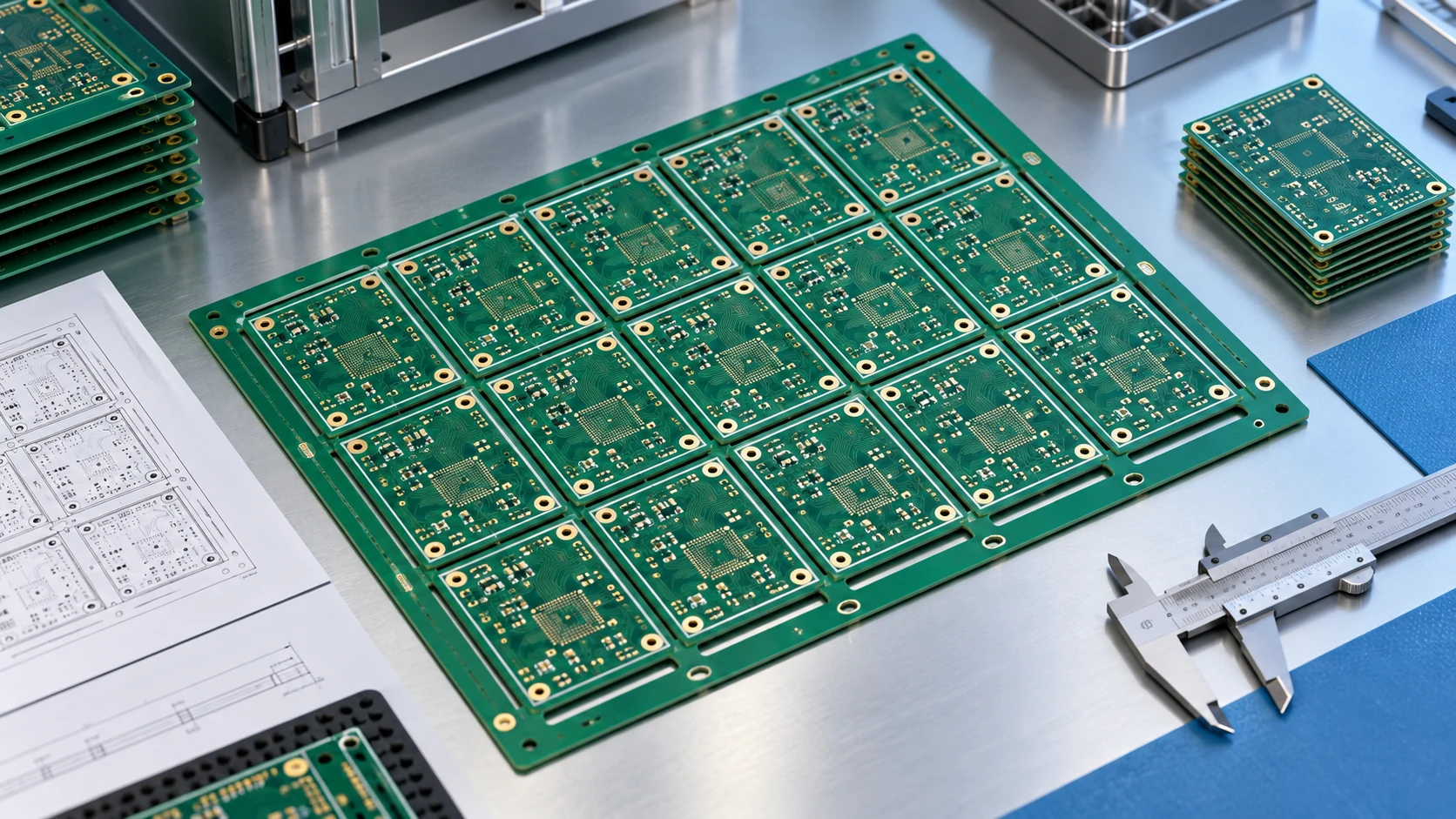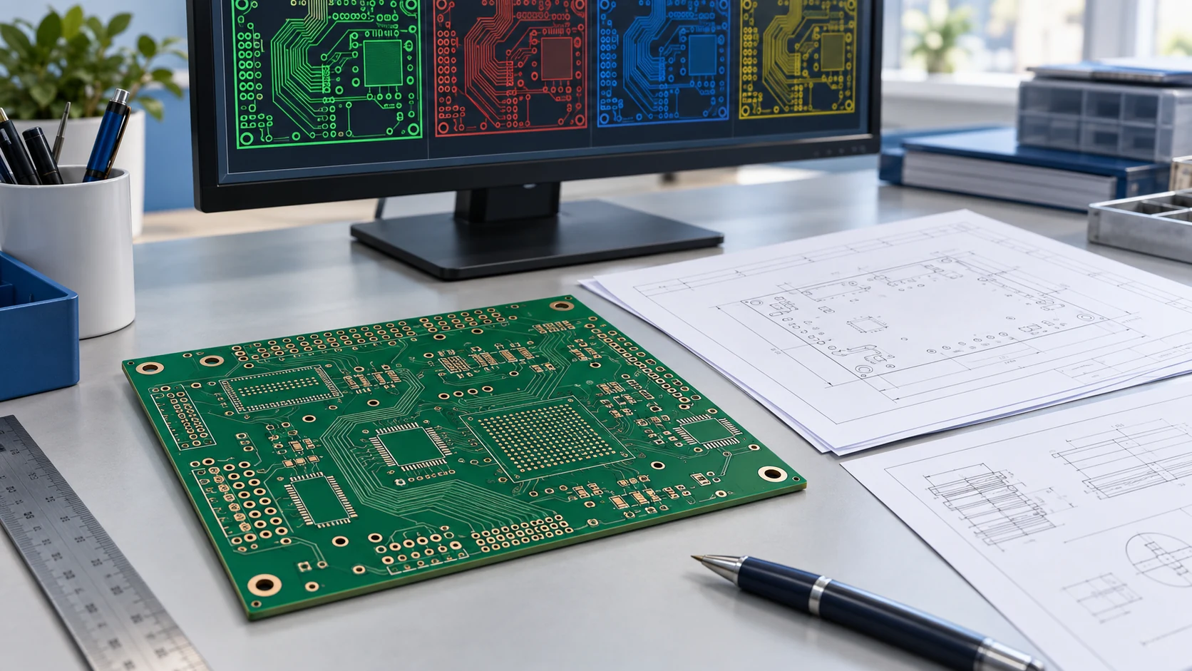

The PCB manufacturing process turns a released circuit design into a tested bare board through a controlled series of imaging, etching, lamination, drilling, plating, finishing, and inspection steps. The exact route depends on layer count, material, via structure, copper weight, surface finish, and the acceptance criteria specified for the order.
For a B2B buyer, knowing the sequence helps explain why a design question at the start can affect yield, price, and delivery later. This guide follows a conventional rigid multilayer PCB from fabrication data to shipment, notes where simpler or advanced constructions differ, and identifies the decisions your team should confirm with a supplier. It describes a typical industry workflow rather than claiming that every order follows identical equipment or checkpoints.
Start with Released Data and a Manufacturing Review
Manufacturing begins before a panel enters the production line. The fabricator receives the released artwork and supporting requirements, identifies the layer sequence, and checks whether the files agree. Copper, solder mask, legend, drill and routing data describe different parts of the board. A fabrication drawing or controlled specification carries requirements that a layer image alone cannot settle, including finished thickness, material, finish, tolerances, and acceptance class.
Ucamco, the steward of the Gerber format, explains that fabrication data must establish each layer's function and its place in the stackup. Its official Gerber documentation is a useful reference for data transfer, but the receiving supplier's accepted file package still governs the order. If your team is preparing an RFQ, use our PCB quotation file checklist to confirm that the artwork, drills, outline, and drawings refer to the same revision.
CAM checks that affect the build
During computer-aided manufacturing review, engineers compare the board outline and panel plan, confirm drill-to-copper relationships, inspect trace and space rules, and identify features that need clarification. They may propose a manufacturable panel, tooling features, or a stackup compatible with the stated impedance targets. These are engineering proposals until the customer approves a change to the released design.
Ask for a written question log when a requirement is ambiguous. The log should identify the drawing or file at issue, the proposed interpretation, the owner of the answer, and whether a revised data package is needed. This prevents an informal email from becoming an undocumented production instruction. The rigid PCB capability page provides published manufacturing parameters, but a specific combination of limits still needs project review.
PCB Manufacturing Process at a Glance
The table below summarizes a typical rigid multilayer route. It is a planning map, not a universal traveler: double-sided boards omit inner-layer lamination, while HDI builds may repeat imaging and lamination with microvia operations.
| Stage | Main purpose | Buyer or engineering checkpoint |
|---|---|---|
| Data and CAM review | Translate released design into a manufacturable job | Approve stackup, exceptions and revision |
| Inner-layer imaging and etching | Form internal copper circuits | Confirm layer order and polarity |
| Inspection and lamination | Verify inner layers and bond the stack | Review material and finished thickness |
| Drilling and hole metallization | Create interlayer connections and mechanical holes | Specify finished hole sizes and via types |
| Outer-layer imaging and plating | Build external circuitry and plated features | Confirm copper and geometry requirements |
| Mask, finish and legend | Protect copper and prepare solderable pads | Specify finish, mask openings and marking |
| Profiling and final test | Separate boards and verify released requirements | Agree test, acceptance and shipment records |
Eurocircuits publishes a detailed step-by-step PCB manufacturing overview that illustrates many of these operations in practice. Production sequence, chemistry, equipment, and inspection points can vary by factory and board construction. Compare the proposed route with the supplier's own process documentation for critical programs.
Image, Etch and Inspect the Inner Layers
For a multilayer board, fabrication commonly starts with copper-clad core material. The inner-layer circuit pattern is transferred to a photoresist using an imaging process. After development, exposed unwanted copper is etched away, leaving the intended conductors and planes. The resist is then removed as specified by the process.
Because these copper features will be buried after lamination, inspection must happen while they remain visible. Automated optical inspection compares the produced image with the expected pattern and helps identify opens, shorts, or geometry defects before the layers are bonded. An AOI result is a process-control signal; it does not replace final electrical testing of the completed board.

Why early control matters
Once layers are laminated, an internal defect may be difficult or impossible to repair. Early checks therefore protect later processing time and material. The controls needed depend on conductor density and reliability requirements; a fine-line high-density design may need a different review from a broad-trace power board.
Buyers should confirm how the supplier identifies each inner layer, keeps revisions separated, and records disposition of any defect found before lamination. If a board mixes fine lines, heavy copper, or unusual material, discuss the tradeoffs at design review rather than assuming all headline capability limits can be combined on the same build.
Laminate the Stack, Then Drill the Board
Approved inner layers are aligned with insulating prepreg and outer copper foils, then bonded under controlled heat and pressure. The laminate construction is chosen to meet the specified layer order, board thickness, material properties, and, when applicable, electrical performance. Registration matters because later drilling must connect the intended pads through the completed stack.
After lamination, mechanical drilling creates through holes for vias, component leads, mounting features, and other approved openings. The drill program must distinguish plated from non-plated holes and reflect the required finished sizes. Tool wear, stack height, material, and hole aspect ratio influence manufacturability. A drawing that gives only a nominal hole diameter without clarifying the finished requirement can lead to different assumptions at quotation and inspection.
What changes for HDI or blind-via designs?
Advanced boards may use laser-drilled microvias, blind or buried vias, and repeated sequential lamination. Those operations are not simply extra holes added after a conventional through-hole route. They alter the stackup, layer registration, process sequence, and reliability review. See the published HDI PCB manufacturing capabilities if your design needs those structures, and submit the actual via architecture for engineering confirmation.
Before approving a stackup or drill plan, check total thickness, copper distribution, dielectric requirements, controlled-impedance targets, and the land size around each via. Ask whether requested tolerances apply to the finished board, the drilled hole before plating, or the routed outline. These distinctions are particularly important for press-fit connectors, fine-pitch interfaces, and assemblies constrained by an enclosure.
Metallize Holes, Pattern Outer Copper and Inspect
Drilling exposes nonconductive hole walls in the laminate. A hole metallization sequence makes the appropriate barrels conductive, and copper plating builds the connection between layers. Outer-layer circuitry is then imaged and patterned; plating and etching form the required external pads and traces. The precise chemistry and sequence depend on the fabricator's process, so the customer-facing requirement should specify finished performance and dimensions rather than prescribing an unreviewed recipe.
Plated-through-hole integrity is a key reliability topic. IPC describes IPC-6012 as a qualification and performance specification for rigid printed boards, including boards with plated through holes and multilayer constructions. IPC-A-600 provides visual acceptability guidance. Name the applicable standard and class in your purchase specification rather than assuming that the same criteria apply to every order.
Control the finished geometry, not just the nominal design
Etching changes conductor dimensions, while plating adds copper to surfaces and holes. The fabricator plans compensation within its process window, but released artwork, copper weight, trace and space, hole size, and tolerances must still be internally consistent. For controlled impedance, the stackup, dielectric data and trace geometry should be reviewed together; a note that says only “50 ohms” is not enough to define all structures and acceptance conditions.
Ask for specific evidence appropriate to the program: coupon or cross-section results where specified, plating records, AOI checkpoints, and approval of any stackup substitution. These records should relate to the manufactured lot and agreed quality plan. A full set of tests is not automatically included in every quotation, so make the required documentation explicit during the RFQ.
Apply Solder Mask, Surface Finish and Board Markings
Solder mask is applied and imaged to leave the intended pads and contact regions exposed while protecting other copper. The mask opening, registration, and clearance around fine-pitch features should agree with the assembly design. Legend or silkscreen markings can then identify components and other approved information, provided the markings do not obstruct pads or conflict with the controlled artwork.
A surface finish protects exposed copper and prepares pads for soldering or contact use. Common choices include HASL, ENIG, OSP, immersion tin, and immersion silver; each has different process and application considerations. Specify the finish in the fabrication package, and confirm whether any connector fingers or special contact areas require a different treatment. Do not let a board drawing and a purchase order name different finishes.
The panel is then routed, scored, or otherwise profiled to the agreed outline and delivery format. The supplier's production panel is not necessarily the same as an assembly panel requested for automated placement. If you need rails, fiducials, tooling holes, tabs, or a V-score arrangement, identify the delivered panel requirement and approve any supplier proposal before production.
Keep fabrication and assembly scope distinct
At this point the result is still a bare PCB. Component sourcing, paste printing, placement, reflow, through-hole insertion, programming, and functional test belong to the PCBA scope. If you are purchasing a populated board, review the SMT assembly services and supply a BOM, placement data, assembly drawings, and test instructions in addition to the bare-board files.
Electrical Test, Final Inspection and Lot Release
Before shipment, the finished bare board is checked against the agreed electrical and visual requirements. An electrical test compares the completed netlist with the expected connections and looks for opens and shorts. Test methods can include flying-probe or fixture-based approaches according to volume, geometry, and the supplier's plan. Passing electrical test does not demonstrate that a future assembled product will function, because components and software are not part of a bare-board netlist check.

Final inspection also considers dimensions, surface condition, solder mask, marking, and other specified acceptance items. More detailed structural verification may be required by the purchase specification or quality plan. IPC's IPC-A-600 guidance covers externally and internally observable printed-board conditions; the agreed class and applicable performance specification determine which criteria govern the order.
Release documents should match the buyer's risk
For a prototype, a clear revision label and test record may be enough to support the next engineering decision. For production or regulated programs, buyers may request lot traceability, inspection reports, certificates, or retained test data. Define these deliverables before production and specify how nonconformances and concessions must be approved.
Packaging is the final control, not an afterthought. The board should arrive identifiable, protected from handling and transport damage, and separated by part number and revision. Receiving teams should be able to match the shipment with the approved purchase order and fabrication revision without reconstructing a trail from informal messages.
What B2B Buyers Should Confirm Before Release
A process description becomes useful when it helps engineering and procurement ask the same questions. Before placing a production order, confirm the following items with the fabricator:
- One released revision: artwork, drill files, outline, drawing, and purchase specification identify the same board.
- Approved construction: layer order, material, copper, finished thickness, and impedance requirements are agreed.
- Clear special features: blind vias, slots, controlled-depth features, edge plating, panelization, and special finishes are explicitly reviewed.
- Acceptance plan: applicable standards, class, electrical test, inspection records, and traceability are documented.
- Commercial scope: quantity breaks, tooling, delivery assumptions, one-time work, and exclusions are visible in the quotation.
The process can change cost as well as lead time. Additional lamination cycles, difficult drilling, tighter geometry, special finishes, and expanded inspection can add work even when two designs have the same dimensions and layer count. Our PCB manufacturing cost guide explains how to compare those quote drivers without treating a nominal board specification as a complete price.
Supplier evaluation is similarly broader than a list of machines. Review engineering responses, revision control, test capability, quality documentation, and communication before committing a repeat program. The B2B PCB manufacturer selection guide provides a structured checklist for that decision.
For a specific project, send the controlled file set and state any open questions. XinshunPCB can review the applicable manufacturing capabilities against your construction and quotation scope. Request a written response to exceptions before approving production.
PCB Products for Different Manufacturing Routes
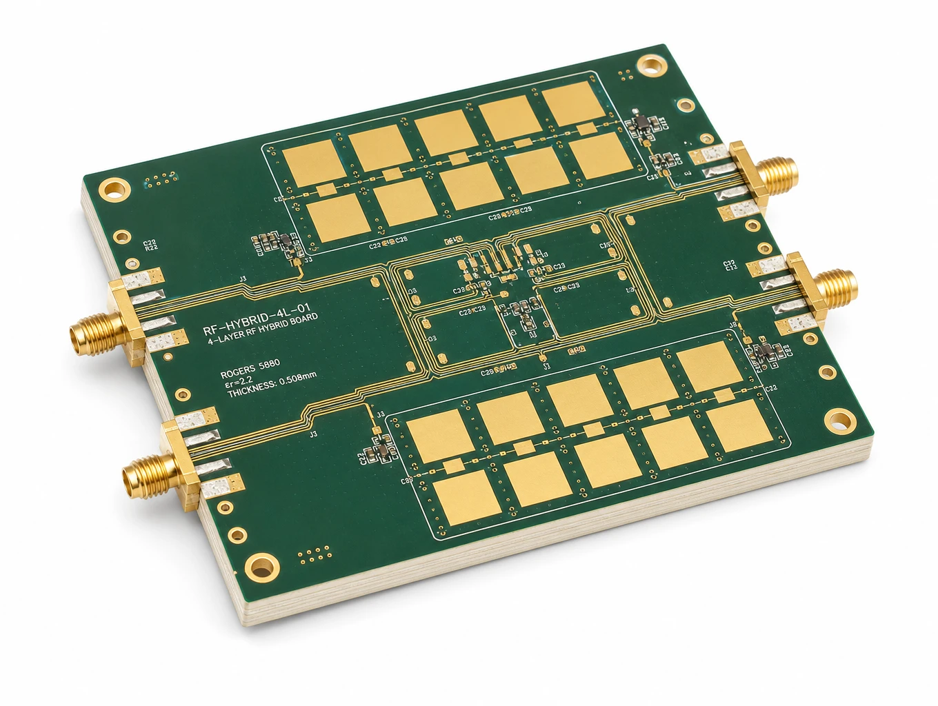
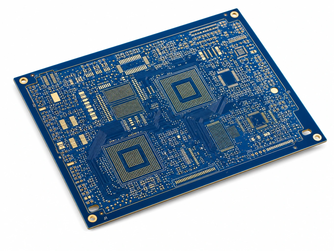
Explore representative board types for rigid multilayer, HDI, and flexible interconnect requirements. The released design and supplier review determine the actual manufacturing route.

PCB Applications That Shape Process Requirements
Application environment, reliability target, and assembly method can change the best material, finish, inspection, and traceability plan.

Industrial & Power Electronics
Engineered to withstand massive electrical currents, thermal stress, and continuous mechanical vibration. XinshunPCB delivers IPC Class 3 heavy copper boards, high-thermal metal-core solutions, and turnkey SMT assemblies for grid-scale energy storage, industrial robotics, motor drives, and solar inverters.
Explore Solutions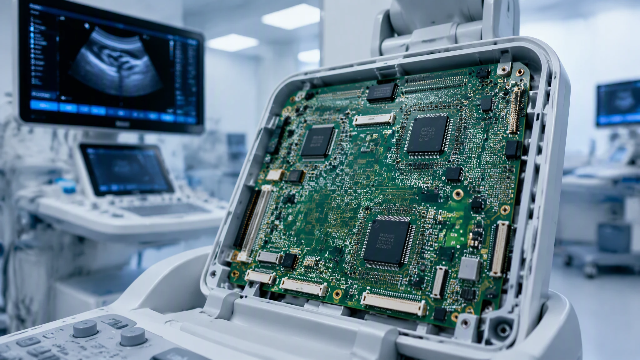
Medical Equipment
From patient monitoring and diagnostic instruments to medical imaging systems, XinshunPCB provides custom PCB fabrication and PCBA assembly for healthcare equipment. We help you align board materials, circuit layouts, and assembly requirements with your application, supporting development from initial prototypes to production.
Explore Solutions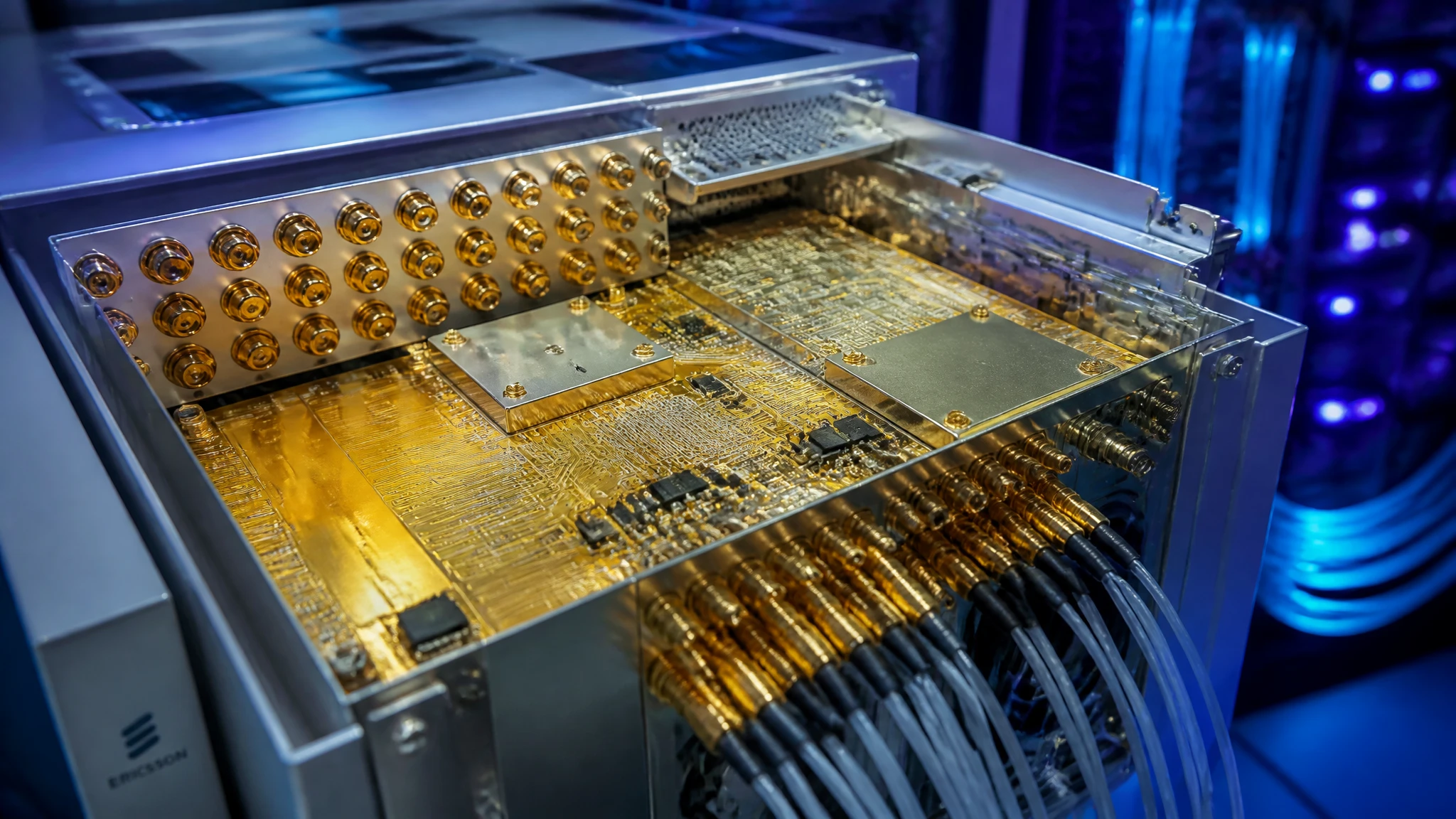
Telecommunications & IoT
From wireless gateways and connected sensors to networking equipment, XinshunPCB supports custom PCB fabrication and assembly for communication hardware. Align materials, stackups, compact layouts, and production testing with your application, from initial prototypes to repeat production.
Explore Solutions Industrial & Power Electronics
Engineered to withstand massive electrical currents, thermal stress, and continuous mechanical vibration. XinshunPCB delivers IPC Class 3 heavy copper boards, high-thermal metal-core solutions, and turnkey SMT assemblies for grid-scale energy storage, industrial robotics, motor drives, and solar inverters.
Explore Solutions Medical Equipment
From patient monitoring and diagnostic instruments to medical imaging systems, XinshunPCB provides custom PCB fabrication and PCBA assembly for healthcare equipment. We help you align board materials, circuit layouts, and assembly requirements with your application, supporting development from initial prototypes to production.
Explore Solutions Telecommunications & IoT
From wireless gateways and connected sensors to networking equipment, XinshunPCB supports custom PCB fabrication and assembly for communication hardware. Align materials, stackups, compact layouts, and production testing with your application, from initial prototypes to repeat production.
Explore SolutionsPCB Manufacturing Process FAQs
Answers to common engineering and purchasing questions about a rigid PCB fabrication route.
Next Step: Review Your PCB Build
The PCB manufacturing process is a linked chain: data review guides the build, imaging and lamination establish the circuits, drilling and plating connect them, and finishing and testing determine whether the delivered board meets the released requirements. The right discussion is therefore not “Can you make a PCB?” but “Can this exact revision, construction, and acceptance plan be manufactured and verified?”
Ready to review a design? Request a PCB manufacturing quote from XinshunPCB with your Gerber or other accepted production data, fabrication drawing, quantities, target schedule, and special requirements. Identify any proposed alternatives so they can be reviewed separately from the released build.
Continue Planning Your PCB Manufacturing Project
These guides connect process decisions with supplier selection, quotation inputs, and total cost.