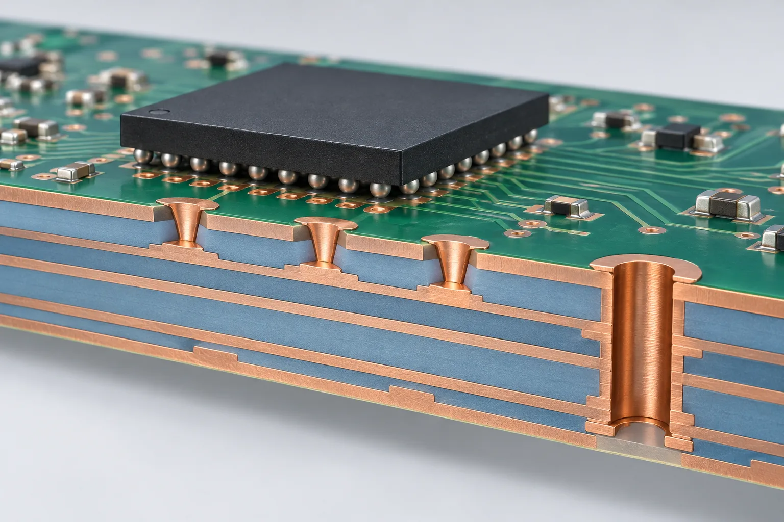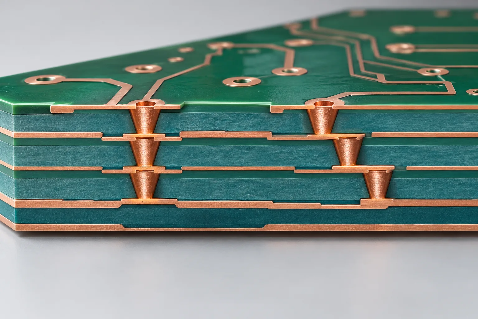

Specify the Finished Pad, Not Just the Via Location
A via-in-pad PCB manufacturer needs more than a drill file with holes inside component lands. The fabrication package must identify the selected vias, their layer spans, the filling method and the copper surface required for assembly. Approve these requirements with both the fabricator and assembler before releasing the design.
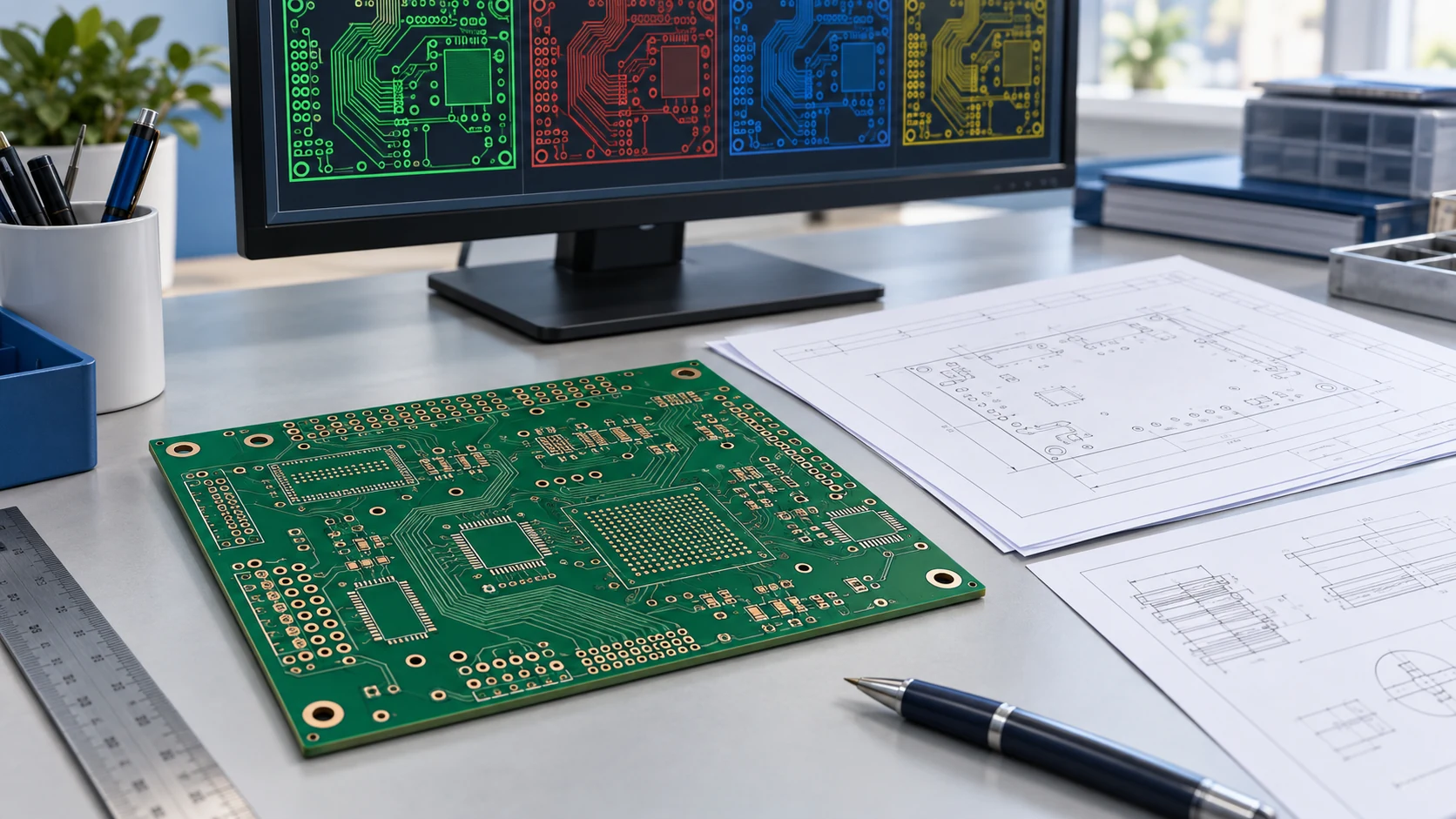
Via-in-pad places an interlayer connection in a component pad rather than beside it. The attraction is straightforward: the connection can occupy less escape-routing space. The challenge is that a pad used for soldering must still provide the surface the assembly process expects. A note saying “plug all vias” may leave that requirement unresolved.
For custom HDI PCB manufacturing, treat via location, hole treatment and solderability as separate decisions. A board can pass electrical continuity testing while its pad surface still fails an agreed assembly requirement. Manufacturing release needs evidence for each relevant property.
- Which via families sit within solderable component pads?
- Does each family need filling, copper capping and a defined surface profile?
- What measurements and acceptance evidence will confirm the result?
- Does the quote include the approved fabrication and assembly scope?
This guide focuses on specifying and buying that construction. Use the broader HDI PCB design guidelines for build-up architecture and routing rules; use the requirements below to close the gap between a CAD feature and a manufacturable soldering surface.
What Does Via-in-Pad Mean on a Manufacturing Drawing?
Via-in-pad describes a location. VIPPO, commonly expanded as via-in-pad plated over, describes a treated construction intended to provide a copper surface over the via. Neither term, by itself, tells the fabricator every dimension, material, inspection requirement or permitted process variation for your board.
Separate the via schedule from the surface-treatment notes. A through via extending across the board and a short blind microvia may both appear inside component pads, but they do not automatically share the same filling route. A supplier should identify the approved construction for each family, including any interfaces created during sequential lamination.
| Drawing term | What it identifies | What still needs agreement |
|---|---|---|
| Via-in-pad | A via located within a component land | Hole span, fill, cap and final solderable surface |
| Tented or mask-covered | Solder-mask treatment over a via opening or area | Whether the required pad remains solderable; this is not a copper cap |
| Plugged | Material penetrates part of a via | Extent of fill and whether additional surface treatment is required |
| Filled | Material occupies the hole according to the specified process | Fill acceptance and any required copper cap |
| Filled and copper-capped | A filled via with a copper cap | Cap continuity, surface profile, finish and acceptance criteria |
Würth Elektronik’s via-treatment design guide distinguishes partial plugging, filling, solder-mask coverage and copper capping. Its IPC-4761 examples identify Type VII as filled and capped. Use the terminology to prevent ambiguity, then agree the applicable document revision and exact construction with your supplier.
Do not substitute “covered” for “capped” in a release note. Ask for a marked cross-section if the terminology differs between the designer, fabrication quotation and assembler. An approved drawing is more useful than assuming everyone interprets an abbreviation the same way.
Choose the Fill Material and Copper-Cap Requirement Together
Choose the filling route for the actual via geometry and intended function, then specify whether a copper cap is required. A resin-filled through via and a copper-filled laser microvia are different constructions. A general “conductive fill” instruction does not establish the material, cap quality or qualified process.
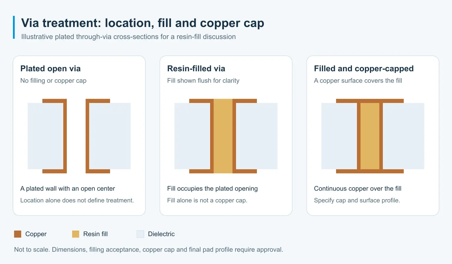
In a resin-filled plated via, the barrel copper provides the established electrical connection; selecting a non-conductive filler does not mean removing that connection. The fill material and cap still need to be suitable for the construction and its assembly exposure. Request the proposed material identification and approval conditions rather than treating the word “epoxy” as a complete specification.
For a copper-filled microvia, ask how the supplier controls filling and the surface on which any subsequent layer connection lands. If successive vias stack above one another, their arrangement adds another review question. The stacked and staggered microvia comparison explains that routing choice without replacing a treatment specification.
Start from XinshunPCB’s HDI filling and VIPPO capabilities, which lists copper-filled and resin-filled, capped and planarized options subject to review. Submit your proposed stackup and via map so the available combination can be confirmed. A capability listing is not blanket approval for every hole, pad or material combination.
For a thermal objective, discuss the complete heat path, including copper geometry, interfaces and the destination for the heat. Filler conductivity alone is not a board-level thermal-performance result. Avoid changing an approved material solely because another filler has a more attractive headline property.
Turn Planarity and Hole Geometry into Inspectable Requirements
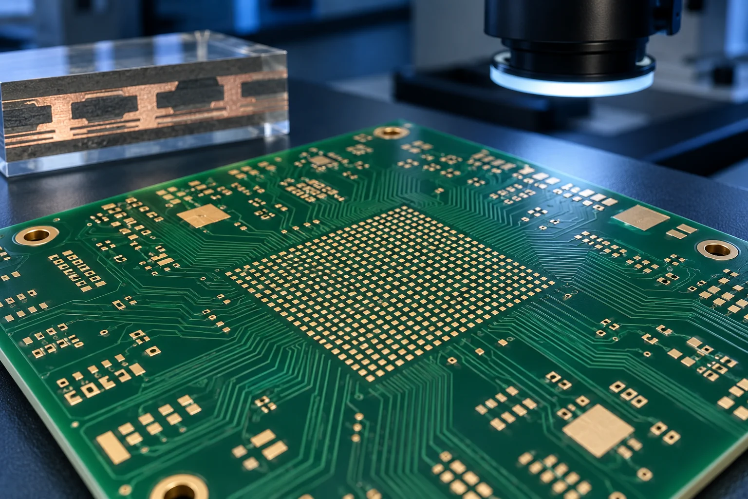
Planarity is a measurable surface requirement, not simply a visual impression of a filled hole. Define the permitted pad profile, the reference surface and the inspection method. The fabricator and assembler should agree what counts as acceptable before a production lot is evaluated.
Ask the supplier how the copper cap is supported and inspected. A depression, projection, discontinuity or exposed fill may matter differently depending on the component and assembly process. Specify the applicable limits in an approved drawing or acceptance document; do not copy a generic internet tolerance into every design.
- Hole definition: distinguish tool diameter, opening diameter and the agreed finished condition.
- Layer span: identify start and end layers for every blind, buried or through-via family.
- Pad geometry: include component land, capture pad, registration allowance and relevant clearances.
- Surface profile: define permitted depression or projection relative to a stated reference.
- Copper and finish: agree cap requirements and the finished solderable surface.
- Inspection: identify measurement technique, sampling and the evidence delivered with the lot.
A surface-finish name does not answer all these questions. For example, naming ENIG does not establish whether the underlying via is appropriately filled, capped or planarized. Keep the geometry and treatment requirements visible alongside the finish specification.
Review these details against the actual multilayer PCB stackup. Hole depth, copper distribution and lamination sequence interact with fabrication choices. Check whether a process proposed for prototypes is also the intended route for repeat production, and record any change that requires renewed approval.
Finally, distinguish sample appearance from acceptance coverage. One attractive microsection image does not establish the sampling plan for every via family or production lot. Ask what the evidence represents, how the inspected features are selected and how results are tied to the board revision.
Review BGA Assembly and Thermal Pads with the Assembler
The relevant question is whether the finished land supports the intended solder joint. Via treatment must be reviewed with the component footprint, solder-mask openings, paste deposition and reflow process. Fabrication approval and assembly approval are related, but one should not be assumed to replace the other.
Texas Instruments’ SPRABB3 package-design report discusses solder movement and trapped gas around untreated vias, and describes filled, planarized and plated-over lands for component attachment. It also emphasizes coordination with fabrication and assembly suppliers. The report is dated June 2010 and concerns particular package constructions; its numerical recommendations are not universal rules for current devices.
Use the current component manufacturer’s land-pattern and assembly recommendations for the selected package. Ask whether the proposed land, mask and paste design remains appropriate above the agreed via treatment. If the team proposes a process change, compare it against the package requirements rather than accepting a bare-board statement such as “the holes are sealed.”
Thermal or exposed pads need their own discussion. Their size, via placement and soldering objectives can differ from individual BGA signal lands. An approved open, offset or filled thermal-via arrangement in one package does not automatically authorize the same treatment inside another package’s small solder lands.
Agree how the first assembly will be evaluated. Define the required visual or X-ray review, electrical checks and any project-specific qualification. These methods answer different questions: an electrical test does not directly measure copper-cap planarity, while an X-ray image should not be treated as a universal substitute for every bare-board inspection.
Where the quotation includes assembly, state who approves the footprint, stencil and inspection criteria. The PCBA inspection and testing guide helps separate AOI, X-ray, ICT and functional testing so the purchasing scope matches the evidence actually required.
Qualify a Via-in-Pad PCB Manufacturer with Comparable Evidence
Qualify a via in pad PCB manufacturer against the construction you need, not a single advertised minimum hole size. Ask for evidence that relates to the proposed material, via family, build-up and assembly exposure. Keep engineering approval separate from a purchasing comparison based only on unit price.
Begin with a construction review. Give each supplier the same stackup, via schedule and selected-fill map, then request a marked response showing accepted features and proposed changes. An unrestricted “yes” is less useful than a clear explanation of which details are approved and which remain provisional.
A practical supplier discussion should cover:
- Process fit: Which via families use resin filling, copper filling or another explicitly approved treatment?
- Surface control: How are fill cure, planarization and cap plating managed for the requested construction?
- Inspection evidence: What microsections, surface measurements and electrical records are included, and what do they sample?
- Assembly compatibility: Has the relevant pad construction been reviewed with the assembler and current component requirements?
- Change control: Which material, process or stackup changes need customer approval?
- Repeatability: Is the prototype construction intended to transfer to the quoted production route?
For demanding service conditions, define a qualification plan with your engineering and quality teams. A capability sheet, generic certificate or unrelated sample photograph cannot prove the service life of your particular board. Identify the construction represented by each test record and the acceptance decision it supports.
Ask for traceability at a useful level. The purchase order, drawing revision, approved deviations and inspection report should refer to the same released configuration. If the supplier presents an alternative construction, record its effect on routing, assembly, qualification, delivery and price before accepting it.
This review also protects schedule. Resolve an unapproved pad profile or ambiguous fill note while the design is still editable. Discovering the disagreement after board fabrication leaves the team choosing between a deviation review, assembly experiment and a new build.
Make Via Treatment Explicit in the RFQ Package
A useful RFQ identifies both the physical via families and the required finished surfaces. Provide a selected-via map when treatments differ across the board. The quotation should refer to the same revision of that map, the fabrication drawing and the assembly requirements.
Eurocircuits’ via-filling data guidance gives separate identification of selected fill holes as a way to communicate intent. It also documents additional fabrication stages for its resin-fill process. The relevant lesson is to specify the selected features clearly; its machines, materials and dimensional limits are not XinshunPCB specifications.
| RFQ item | What to provide | Decision it enables |
|---|---|---|
| Manufacturing data | Gerber or agreed intelligent data format, drill information and board outline | Confirm the released geometry and data interpretation |
| Stackup and via schedule | Numbered layers, via families, spans and dimensional definitions | Match each via family to a manufacturing route |
| Treatment selection | A marked layer/file or agreed map identifying vias requiring fill and cap | Avoid filling mounting or component-lead holes by mistake |
| Material and surface notes | Agreed filler, copper cap, surface-profile and finish requirements | Review the finished solderable land |
| Assembly information | Package references, land pattern, mask/paste data and assembler requirements | Check fabrication-to-assembly compatibility |
| Acceptance and qualification | Applicable revisions/classes, measurements, sampling and agreed tests | Make inspection scope comparable |
| Commercial release | Quantities, prototype/production scope, delivery assumptions and revision control | Compare quotations on the same basis |
A useful drawing note might read: “Vias identified in the approved treatment map require the specified fill, copper cap and surface profile. Supplier to confirm the material, inspection method and acceptance limits against drawing revision X before manufacture.” Replace the placeholders with agreed values and documents; this example is a communication checklist, not a ready-to-use acceptance specification.
For the wider file package, follow the PCB and PCBA quotation file checklist. Keep one revision-controlled release folder and remove superseded files before sending it. If a fabricator returns edited manufacturing data, approve and archive the changed revision explicitly.
Compare Cost and Release the Approved Construction
Compare quotations for the same via treatment, evidence and production scope. Filling, cure, surface preparation, cap plating and inspection can affect the process route. The cost effect depends on the board and supplier; a fixed percentage uplift is not a reliable purchasing rule.
Where routing permits, ask the team to compare a conventional connection beside the pad with the proposed via-in-pad construction. This is an engineering alternative to evaluate, not an instruction to move every via. A change can affect routing density, layer count, electrical behavior and assembly needs, so include those consequences in the comparison.
Separate recurring board price from setup, qualification, test coupons and any assembly-development work. A lower unit price may omit evidence another supplier has included. The PCB manufacturing cost guide explains how materials, layers, geometry and production assumptions change quotation scope.
Before release, reconcile the supplier’s DFM response with the purchase documents. Confirm the final via schedule, material, cap and profile requirements, approved deviations, assembly responsibilities and inspection deliverables. Ensure the same decisions reach engineering, quality and procurement.
Do not close a technical query with a vague commercial approval. If a supplier offers a different filler or cap construction, record who reviewed the change and whether qualification or assembly checks need to be repeated. Keep the approved revision identifiable when the project moves from an initial build to repeat orders.
The goal is a clear manufacturing agreement: a specific construction, a compatible soldering surface and evidence appropriate to the intended application. That is a stronger basis for supplier selection than a generic VIPPO label or an isolated minimum-feature claim.
HDI PCB Examples for a Via-in-Pad Review
Review these published construction examples with your own via schedule and assembly requirements. Each project needs its own manufacturing approval.


Applications with Dense Component and Interconnect Requirements

Consumer Electronics
Bring connected consumer products from prototype to production with XinshunPCB. We support custom PCB fabrication and SMT assembly for wearables, smart-home devices, wireless audio and portable electronics, with material, component and test requirements reviewed around your design.
Explore Solutions
Medical Equipment
From patient monitoring and diagnostic instruments to medical imaging systems, XinshunPCB provides custom PCB fabrication and PCBA assembly for healthcare equipment. We help you align board materials, circuit layouts, and assembly requirements with your application, supporting development from initial prototypes to production.
Explore Solutions
Telecommunications & IoT
From wireless gateways and connected sensors to networking equipment, XinshunPCB supports custom PCB fabrication and assembly for communication hardware. Align materials, stackups, compact layouts, and production testing with your application, from initial prototypes to repeat production.
Explore Solutions Consumer Electronics
Bring connected consumer products from prototype to production with XinshunPCB. We support custom PCB fabrication and SMT assembly for wearables, smart-home devices, wireless audio and portable electronics, with material, component and test requirements reviewed around your design.
Explore Solutions Medical Equipment
From patient monitoring and diagnostic instruments to medical imaging systems, XinshunPCB provides custom PCB fabrication and PCBA assembly for healthcare equipment. We help you align board materials, circuit layouts, and assembly requirements with your application, supporting development from initial prototypes to production.
Explore Solutions Telecommunications & IoT
From wireless gateways and connected sensors to networking equipment, XinshunPCB supports custom PCB fabrication and assembly for communication hardware. Align materials, stackups, compact layouts, and production testing with your application, from initial prototypes to repeat production.
Explore SolutionsVia-in-Pad Manufacturing and Filling FAQs
Practical answers about VIPPO, fill materials, solderable surfaces and the documents needed for a manufacturing review.
Via-in-pad identifies a via located within a component land. VIPPO commonly refers to via-in-pad plated over: a treated construction providing a copper surface above the via. The abbreviation does not specify every material or tolerance. Define the via family, filling route, cap, surface profile and acceptance requirements in the approved fabrication package.
Request a Via-in-Pad Construction Review
Release via-in-pad requirements as a coordinated fabrication and assembly decision. Identify the selected holes, agree the filling and cap construction, define the finished pad and specify the evidence needed for acceptance. Keep those decisions in the same revision-controlled package used for quotation and purchasing.
Send XinshunPCB your via-in-pad files for a project-specific manufacturing review. Include the proposed stackup, via map, pad requirements and quantities so the discussion can address your actual HDI design.