
Start HDI PCB Design with the Actual Routing Problem
HDI PCB design guidelines should connect the component escape plan, layer stackup, microvia geometry and acceptance requirements before layout is frozen. Start with the simplest construction that can route the real device. Then have the fabricator review the layer transitions, via treatment and materials as one build.
For teams sourcing custom HDI PCB manufacturing, the useful question is which connections require build-up layers and why. A label such as “any-layer” does not specify a complete manufacturing route. This guide helps hardware engineers and technical buyers prepare that discussion and compare quotations on the same basis.
- Translate 1+N+1 or 2+N+2 into numbered copper layers and approved via spans.
- Review the actual BGA footprint, connected balls and routing channels.
- Specify via filling, surface requirements and verification evidence.
- Release the approved stackup and fabrication data together.
What Do 1+N+1, 2+N+2 and Any-Layer Mean?
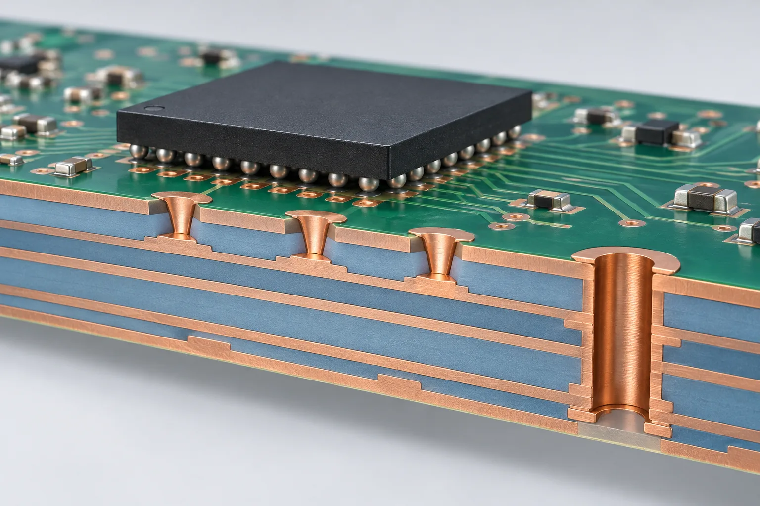
In common symmetric build-up notation, N represents the central multilayer core and the outside numbers describe build-up layers on each side. Thus 1+4+1 describes six copper layers, while 2+4+2 describes eight. These examples describe construction families; a numbered stackup and via map must define the actual connections.
| Construction | What the notation tells you | What still needs approval |
|---|---|---|
| 1+N+1 | One build-up layer on each side of the central core | Outer-to-adjacent-layer access, core connections and routing capacity |
| 2+N+2 | Two build-up layers on each side | Stacked or staggered paths, filling requirements and process sequence |
| 3+N+3 | Three build-up layers on each side | Whether the extra build-up stages are justified by the escape plan |
| Any-layer / ELIC | An interconnect architecture allowing connections through successive layer pairs | The particular layer spans, microvia stacks and qualified manufacturing route |
Würth Elektronik’s HDI technology overview distinguishes sequential build-up, stacked or staggered microvias, and every-layer interconnect architectures. In an any-layer design, a connection across several layers is normally implemented through a defined sequence of interconnections. The name does not mean one laser hole can simply be drilled through the entire board.
Ask the supplier to draw the proposed sequence. For an illustrative 1+4+1 build, show the six numbered copper layers, the two surface microvia spans and any core via. Check where each dense component signal can leave the package and where it reaches its destination. If a signal needs another transition, document that path explicitly.
Build a Via Map Before Setting Minimum Design Rules
Define every via family by its start layer, end layer, hole geometry, pad geometry and treatment. Separate laser microvias from mechanically drilled blind, buried and through vias. The manufacturing sequence determines which internal surfaces are accessible when each hole is formed; the CAD layer span alone is insufficient.
Altium’s microvia design guidance describes the relationship between dielectric thickness, hole diameter and via reliability. Review depth-to-diameter aspect ratio using the agreed geometry definition. A through-hole aspect-ratio limit must not be reused as a microvia limit. Keep capture-pad, registration and fill tolerances in the same review.
Use XinshunPCB’s HDI manufacturing capabilities as an initial discussion reference. The page lists a 0.1 mm laser microvia reference, approximately 0.25 mm capture pads and 3 mil line/space planning values. Confirm the combination for the actual copper, dielectric, via span and production scope; these figures are not an automatic approval of a finished design.
A useful via schedule identifies whether the hole dimension is a drill, opening or finished value. It also identifies the pad on each layer and the permitted stack arrangement. Have the fabricator return an approved schedule or marked drawing before replacing the provisional CAD rules with production rules.
How Should BGA Escape Routing and Via-in-Pad Be Reviewed?
Choose the construction from the actual ball map, connected signals and available routing channels. Ball pitch alone cannot determine the required number of HDI build-up layers. Review package land recommendations, reference continuity, power access and assembly needs before changing pad sizes or adding another microvia stage.
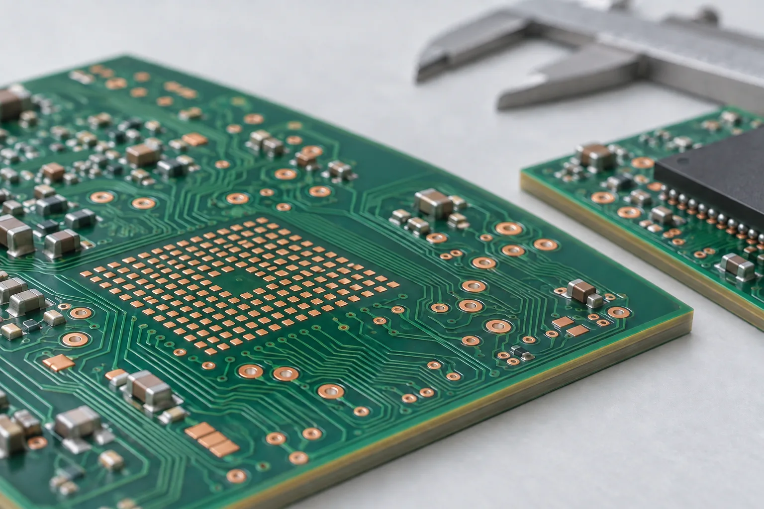
Texas Instruments’ AM570x escape-routing guide provides a device-specific example where package arrangement, via dimensions, pad dimensions and routing priorities are considered together. It explains that different pin-function choices can require different escapes. Use the application note for the actual component; another device’s successful fan-out is not proof that your board can use the same construction.
Würth Elektronik’s HDI design guide shows several escape approaches for the same BGA pitch and relates the required stackup to component complexity. Treat these as examples of tradeoffs. They do not provide a universal pitch-to-layer-count rule or replace XinshunPCB’s approved process values.
If vias sit in component lands, specify the intended filling, capping and planarization treatment and the required solderable surface. An open hole, a filled laser microvia and a resin-filled plated-over through via are different constructions. Confirm the treatment with both fabrication and assembly teams, including any surface depression or protrusion acceptance requirements.
Coordinate Materials, Copper and Impedance with the Build-Up
Review the complete stackup alongside the via map. For each dielectric interval, record the material, proposed finished thickness and relevant electrical properties. For each copper layer, distinguish its starting and finished requirements. A material trade name or Tg value alone leaves the construction and signal environment incomplete.
Use the multilayer PCB stackup checklist to organize layer functions and reference planes. Then add HDI-specific via spans and build-up details. Track the reference path when a critical signal changes layers, and include the impedance target, permitted tolerance, geometry and measurement scope in the release.
The FR-4 material selection guide explains the broader material discussion. For an HDI RFQ, also ask whether the proposed laminate system and dielectric thickness suit the reviewed fabrication and assembly route. Record permitted substitutions and who must approve them before production.
Keep fine routing and copper thickness decisions linked. See the PCB copper thickness guide for specifying copper weight separately from board thickness. Do not combine a fine-line reference from one process with a heavy-copper reference from another and assume the combined design has been approved.
What Evidence Should Support Microvia Reliability?
Match the evidence to the exact construction and intended exposure. A connectivity check at one point in time does not establish that every interconnect will remain sound through assembly and service. Ask which representative structures are tested, under what conditions, and against which agreed acceptance criteria.
IPC’s 2019 warning on microvia reliability reported failures that appeared after boards had passed traditional production acceptance. It highlighted weak microvia interfaces and the limits of relying on conventional microsection inspection alone. The warning is historical evidence for a focused acceptance discussion, not a claim that every stacked-microvia design will fail.
For stacked or more complex structures, request construction-specific qualification evidence and discuss performance-based testing where appropriate. Agree the coupon representation, conditioning or reflow exposure, electrical monitoring, sampling and acceptance criteria before ordering. Ask what happens if a proposed material or process change falls outside the evidence supplied.
Keep bare-board fabrication acceptance separate from assembled-board functional testing. Record the approved revision, material construction and test scope with the build. If a fault appears after assembly, retain the affected board and process history so the teams can investigate the relevant interconnect rather than changing several variables at once.
Prepare an HDI RFQ That Suppliers Can Quote Consistently
Send one controlled release package with a numbered stackup, via map and clear commercial quantities. Ask each supplier to identify assumptions and exceptions in its response. A quotation based on a different via treatment or verification scope should be resolved before its price is compared with another offer.
| RFQ input | What to include | Question to resolve |
|---|---|---|
| Fabrication data | Gerber or ODB++, drill data, outline and one revision identifier | Do the drawings and data describe the same board? |
| Stackup and via schedule | Copper layers, dielectric intervals, layer spans and stack arrangement | Which construction and process route is being quoted? |
| Dense component area | Package reference, ball map, proposed land pattern and escape detail | Can the critical nets route with the approved features? |
| Materials and finish | Material requirements, copper, impedance and solderable surface | Which substitutions or tolerances need written approval? |
| Via treatment and acceptance | Fill/cap/planarization locations, inspection and agreed test evidence | Which records are included with the delivered lot? |
| Order and assembly scope | Prototype and production quantities, delivery needs, BOM and placement files if assembled | What changes between prototype approval and repeat production? |
The PCB quote file checklist covers the base documentation. Add an HDI-specific exception list so unresolved details are visible. For example, if the supplier proposes a staggered connection instead of a stacked one, return that change to the layout owner and approve a revised via map before fabrication.
Compare quotations by separating tooling or setup, board construction, via treatment, required inspection and any assembly service. Request a written explanation when the recommended structure changes. Evaluate whether the proposed simplification still satisfies the routing and acceptance requirements, rather than selecting a layer-count label in isolation.
Request an HDI Stackup and Manufacturing Review
Bring the component escape detail, stackup and via schedule into the same review before releasing the production artwork. Close open assumptions in writing and retain the approved construction with the final revision. Prototype results are most useful when the next order can be traced to that same definition.
XinshunPCB can review an HDI fabrication request against the submitted design and agreed requirements. Request an HDI PCB design and quotation review with your fabrication package, target quantities and acceptance needs. Identify any stacked microvias, via-in-pad areas or proposed any-layer construction in the enquiry so they can be assessed explicitly.
HDI PCB Design and Microvia FAQs
Answers about choosing HDI structures, defining microvias and preparing a manufacturing quotation.
HDI Construction Examples for Your Design Review
Compare selected construction examples, then confirm the appropriate stackup and requirements for your own design.