
Specify Copper and Board Thickness Separately
This PCB copper thickness guide helps OEM engineers and B2B buyers turn a copper-weight requirement into a manufacturable rigid PCB specification. Copper thickness affects resistance, etching and layer construction; finished board thickness affects mechanical fit and drilling. Approving one without the other can leave important gaps in a fabrication quote.
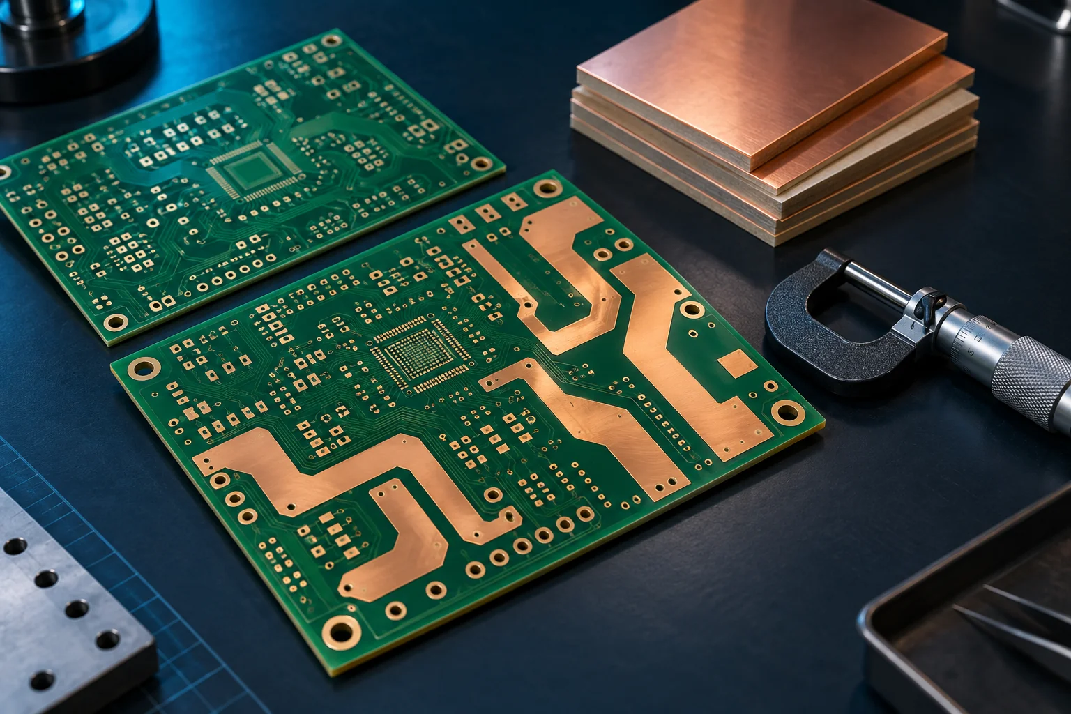
Start with the circuit requirements and the complete layer stack. Decide which layers need additional copper, how the design will remove heat, and what dimensions the assembly must meet. Then agree the finished construction and inspection basis with the fabricator. A generic note such as “2 oz, 1.6 mm” is a starting point, not a complete drawing.
Use rigid PCB manufacturing services as the commercial starting point, and review the PCB stackup design guide when assigning copper to individual layers.
Copper Weight Conversion: Ounces to Micrometres
PCB copper weight expresses mass per unit area, conventionally ounces per square foot. It is not the weight of the whole board. One ounce per square foot corresponds to approximately 34.8 micrometres of copper, commonly rounded to 35 µm in industry discussions. The following values are nominal conversions, not guaranteed finished minimums.
| Nominal copper weight | Approximate thickness | Approximate mils |
|---|---|---|
| 0.5 oz/ft² | 17.4 µm | 0.69 mil |
| 1 oz/ft² | 34.8 µm | 1.37 mil |
| 2 oz/ft² | 69.6 µm | 2.74 mil |
| 3 oz/ft² | 104.4 µm | 4.11 mil |
| 4 oz/ft² | 139.2 µm | 5.48 mil |
| 6 oz/ft² | 208.8 µm | 8.22 mil |
Keep the unit and the manufacturing stage beside each value. A purchase requirement should distinguish a nominal foil designation from an agreed finished copper requirement. If acceptance depends on a minimum thickness, specify its measurement basis and applicable requirements rather than relying on a rounded conversion.
Eurocircuits’ copper thickness guidance explains the conversion and the distinction between incoming foil and finished copper. Its process-specific tolerances should not be treated as universal supplier limits.
Base Copper vs Finished Copper
Base copper is the starting foil on the laminate. Finished copper is what remains after the relevant fabrication operations. On plated outer layers, deposition adds copper while preparation and etching can remove material. Inner layers typically follow a different process route. A single copper-weight note therefore does not describe every layer equally.
Ask whether the quotation describes starting foil, finished conductor thickness, or a minimum accepted thickness. Record inner and outer requirements separately. Also separate planar conductor copper from copper in plated hole walls: specifying a thick surface conductor does not automatically establish the barrel thickness of every via.
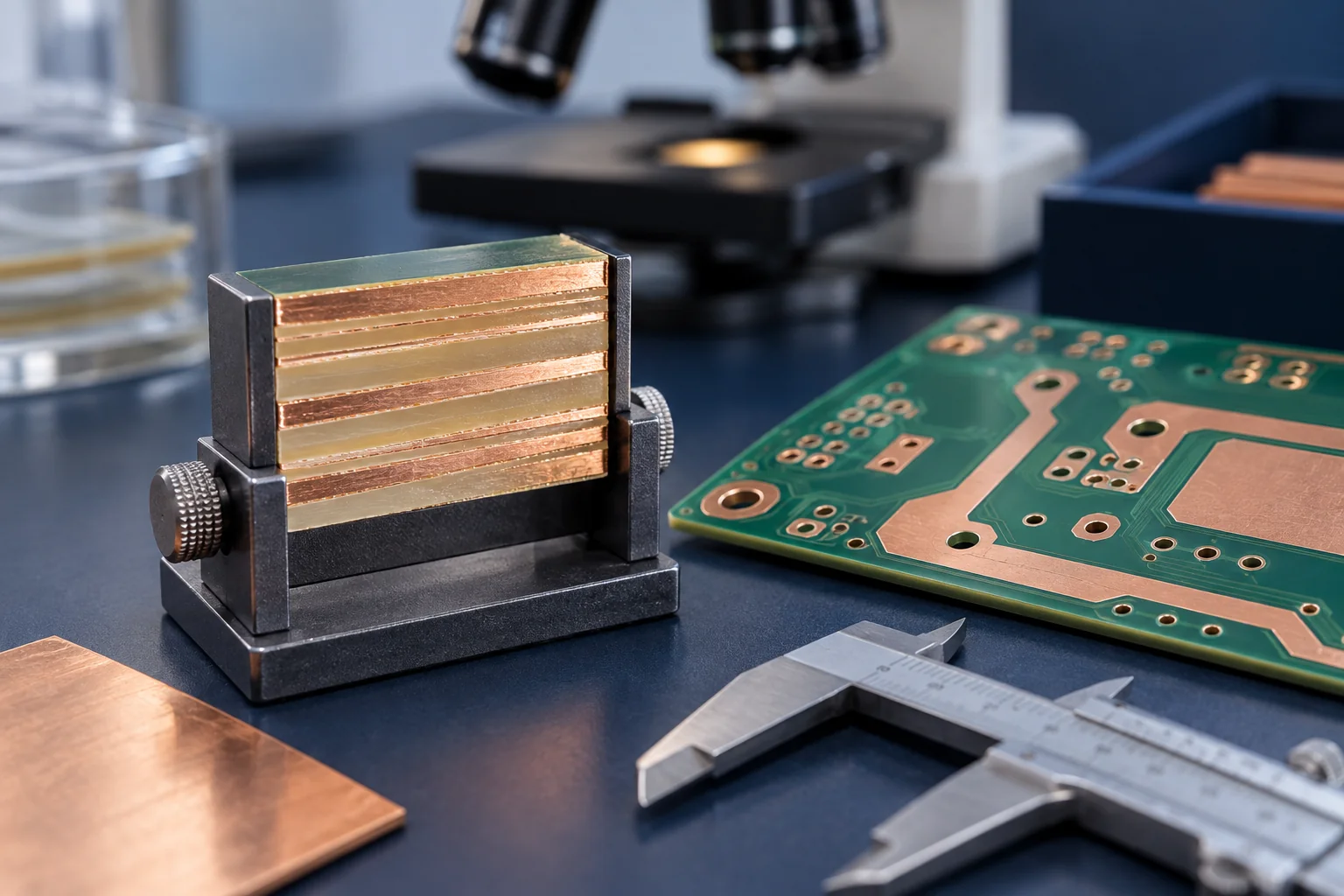
For controlled drawings, agree what evidence is required, such as the approved stackup and specified coupon or inspection records. Do not request an arbitrary measurement on every board without considering sampling, test locations and the acceptance standard. A useful inspection requirement is specific enough for both buyer and manufacturer to apply consistently.
What Thicker Copper Changes in Electrical Design
For the same trace length, width and temperature, increasing conductor thickness reduces DC resistance. In the simple relationship R = ρL/(wt), doubling thickness approximately halves resistance if the other quantities stay unchanged. That relationship does not mean allowable current automatically doubles.
Temperature rise depends on heat transfer as well as electrical loss. Consider internal versus external layers, nearby copper planes, airflow, enclosure conditions, connected pads, neck-downs and thermal paths. Vias, connectors and component terminals can become bottlenecks even when a broad trace uses heavy copper.
Review the worst operating condition with a suitable current and thermal design method, then validate the assembled product when required. Avoid selecting an ounce value from a universal amps-per-ounce table. A copper requirement should follow the permitted temperature rise and circuit geometry, rather than substitute for them.
High-speed design adds another check: finished conductor geometry and dielectric spacing affect impedance. Revisit the proposed stackup when changing copper weight, instead of assuming the original trace widths will still meet the same target.
Heavy Copper and Manufacturability
Heavy copper introduces tradeoffs between power handling and fabrication geometry. Removing a thicker copper layer changes the etching challenge, particularly where fine features and small isolation gaps sit beside wide power regions. Review the design rules for the actual copper construction rather than transferring fine-line rules from a thinner foil.
Eurocircuits’ design classification guidance illustrates why starting foil thickness is linked to allowable conductor and isolation geometry. Those published rules describe that supplier’s process; obtain the corresponding project limits from your chosen fabricator.
- Trace and spacing: confirm the minimum features on each copper layer, especially fine-pitch fan-out beside power circuitry.
- Layer construction: review resin fill and dielectric spacing around thick copper features.
- Copper distribution: assess large differences in copper coverage between regions and layers.
- Assembly interfaces: check solder mask, pads, thermal reliefs and the intended soldering process.
- Cost and delivery: confirm material availability and the approved process before release.
XinshunPCB’s rigid PCB manufacturing capabilities provide a starting point for the engineering review. Published maxima do not mean all maximum parameters can be combined in one board. Request confirmation for the selected copper, feature sizes, hole geometry and layer count together.
Finished Board Thickness and Hole Geometry
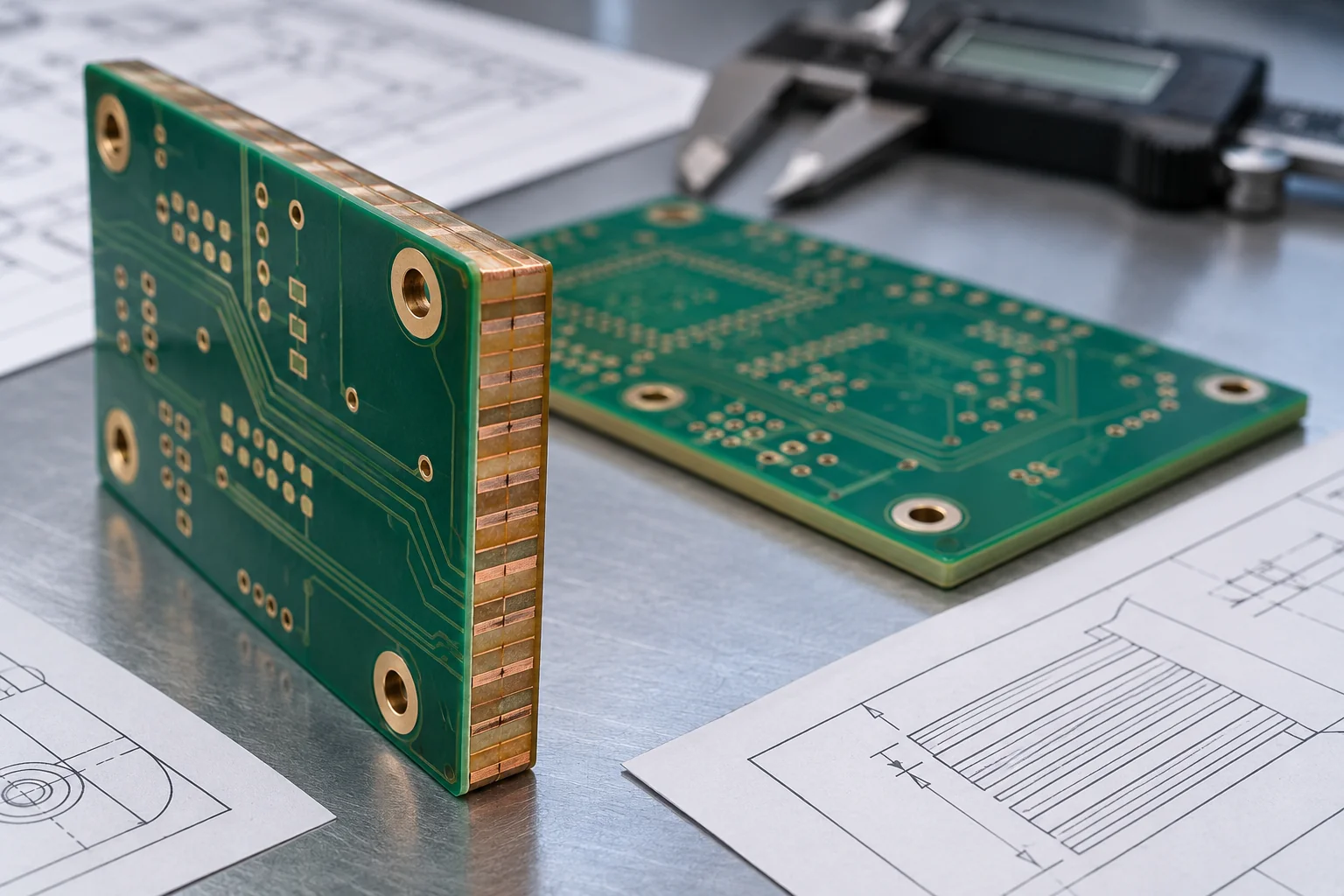
Finished board thickness includes the approved laminate construction and the applicable finished-board definition. It is a separate requirement from copper weight. Specify the target, tolerance and any mating connector or mechanical constraints. A nominal 1.6 mm board is common, but it is not the right thickness for every application.
Increasing board thickness while keeping a small drilling tool increases the through-hole aspect ratio. As an illustration, 1.6 mm divided by a 0.3 mm drill diameter is approximately 5.3:1; 3.2 mm with the same drill is approximately 10.7:1. These are geometric examples, not XinshunPCB process limits. Confirm whether the supplier’s ratio uses manufacturing drill size and how plated finished-hole dimensions are specified.
Review plating access, registration and the intended via structure with the manufacturer. If the design requires a thicker board, consider whether holes, clearances or layer construction need to change. For laminate thermal properties and permitted substitutions, consult the high-Tg FR-4 material selection guide alongside the thickness review.
A B2B Copper Thickness RFQ Checklist
Release a layer-by-layer requirement so purchasing can compare quotations on the same basis. Resolve conflicts between artwork notes, stackup files and mechanical drawings before order placement.
| RFQ item | Information to supply | What to confirm |
|---|---|---|
| Copper per layer | Inner and outer layer weights or thickness requirements | Base versus finished definition; agreed acceptance basis |
| Finished board thickness | Target, tolerance and mechanical constraints | Approved construction and measurement definition |
| Geometry | Smallest traces, gaps, drills and finished holes | Compatibility with the selected copper and board thickness |
| Electrical requirements | Current assumptions, thermal constraints and impedance targets | Any stackup or feature changes required |
| Materials and finish | Required laminate, permitted alternatives and finish | Availability and approval before substitutions |
| Quality records | Applicable standard, inspection scope and documentation | Sampling and evidence included in the quotation |
| Commercial scope | Quantity, revisions, delivery needs and repeat-order forecast | Material and processing assumptions behind price |
For the full design package, use the PCB quotation file checklist. When comparing options, the PCB manufacturing cost guide explains why copper and construction should be evaluated alongside other quotation drivers.
Request a Copper and Stackup Manufacturing Review
Specify additional copper where the design needs it, and check the resulting fabrication and assembly constraints before release. Wider conductors, different layer assignments and improved thermal paths may also address the design objective. Compare the complete alternatives instead of automatically increasing copper on every layer.
Send XinshunPCB the current fabrication package, copper requirements per layer, board thickness, critical features and operating constraints. Identify which parameters are mandatory and which may be adjusted during engineering review. Ask for an approved stackup and a clear record of any changes so subsequent orders use the same construction.
Request a project-specific copper thickness and rigid PCB quote to review your design before production.
PCB Copper Thickness and Heavy Copper FAQs
Answers to common questions about copper weight, finished thickness, current and preparing a fabrication quote.